Showing posts with label digital. Show all posts
Showing posts with label digital. Show all posts
Tuesday, November 4, 2014
Simple But Digital Fan Regulator
The circuit presented here can be used to control the speed of fans using induction motor. The speed control is nonlinear, i.e. in steps. The current step number is displayed on a 7-segment display. Speed can be varied over a wide range because the circuit can alter the voltage applied to the fan motor from 130V to 230V RMS in a maximum of seven steps.
The triac used in the final stage is fired at different angles to get different voltage outputs by applying short-dura-tion current pulses at its gate. For this pur-pose a UJT relax-ation oscillator is used that outputs sawtooth waveform. This waveform is coupled to the gate of the triac through an optocoupler (MOC3011) that has a triac driver output stage.
The triac used in the final stage is fired at different angles to get different voltage outputs by applying short-dura-tion current pulses at its gate. For this pur-pose a UJT relax-ation oscillator is used that outputs sawtooth waveform. This waveform is coupled to the gate of the triac through an optocoupler (MOC3011) that has a triac driver output stage.
Pedestal voltage control is used for varying the firing angle of the triac. The power supply for the relaxation oscillator is derived from the rectified mains via 10-kilo-ohm, 10W series dropping/limit-ing resistor R2. The pedestal voltage is derived from the non-filtered DC through optocoupler 4N33. The conductivity of the Darlington pair transistors inside this optocoupler is varied for getting the pedestal voltage.
For this, the positive sup-ply to the LED inside the optocoupler is connected via different values of resistors using a multiplexer (CD4051).
For this, the positive sup-ply to the LED inside the optocoupler is connected via different values of resistors using a multiplexer (CD4051).
Digital Fan Regulator Circuit Diagram:
![Regulator]()
The value of resistance selected by the multiplexer depends upon the control in-put from BCD up-/down-counter CD4510 (IC5), which, in turn, controls forward bi-asing of the transistor inside optocoupler 4N33. The same BCD outputs from IC5 are also connected to the BCD-to-7-seg-ment decoder to display the step number on a 7-segment display. NAND gates N3 and N4 are config-ured as an astable multivibrator to produce rectangular clock pulses for IC5, while NAND gates N1 and N2 generate the active-low count enable (CE) input using either of push-to-on switches S1 or S2 for count up or count down operation, respectively, of the BCD counter.
Optocoupler 4N33 electrically isolates the high-voltage section and the digital section and thus prevents the user from shock hazard when using switches S1 and S2. BCD-to-7-segment decoder CD4543 is used for driving both common-cathode and common-anode 7-segment displays. If phase input pin 6 is ‘high’ the decoder works as a common-anode decoder, and if phase input pin 6 is ‘low’ it acts as a common-cathode decoder. Optocoupler 4N33 may still conduct slightly even when the display is zero, i.e. pin 13 (X0, at ground level) is switched output pin 3. To avoid this problem, adjust preset VR1 as required using a plastic-handled screwdriver to get no output at zero reading in the display.

Sunday, October 26, 2014
Digital visitor counter
Digital visitor counter is a reliable circuit that takes over the task of counting Number of Persons/ Visitors in the Room very Accurately. When somebody enters into the Room then the Counter is Incremented by one and when any one leaves the room then the Counter is Decremented by One. The total number of Persons inside the Room is displayed on the seven segment displays. The microcontroller do the above job it receives the signals from the sensors, and this signals operated under the control of software which is stored in ROM.
 |
| Digital visitor counter |
 |
| Digital visitor counter |
Sunday, September 21, 2014
Alarm Equipped Digital Clock LM5860 circuit and explanation
Alarm Equipped Digital Clock LM5860 circuit and explanation
LM8560 digital clock circuit has many features like:
- Single chip P-channel ED MOS LSI.
- LED direct drive using time division (duplex configuration).
- Wide operating power supply voltage range.
- Built-in alarm function with 24-hour control.
- Supports changeover between 12-hour AM/PM and 24-hour displays
- Built-in battery backup CR oscillator.
- Built-in automatic fast forward function for hour and minute settings.
- Built-in sleep timer function (maximum intervals of 59 minutes or 1 hours and 59 minutes).
- Built-in snooze function supporting repeat use.
- Equipped with power failure display function.
- 900Hz output for alarm tone .


Using LM8560 circuit you will have many advantages , because of integration in one package of all features you can use it in small clock alarm radio circuits or in a simple clock alarm circuit. For LM 8560 clock alarm circuit you can use a positive or negative power supply maximum 15 volts.
Tuesday, September 9, 2014
4x100W FOUR CHANNEL CLASS T DIGITAL AUDIO AMPLIFIER
General Description:
The TAA4100 is a four-channel Audio Amplifier that uses Tripath’s proprietary Digital Power
Processing (DPPTM) technology. Class-T amplifiers offer both the audio fidelity of Class-AB and the power efficiency of Class-D amplifiers. The TAA4100 has been designed specifically for automotive head unit applications and is configured with four bridged outputs operating on a single 10-26V supply.
Applications:
- Automotive Head Units
- Automotive Amplifiers
- DVD Receivers
- Multimedia Speaker Systems
Benefits:
- 4-channel (400W) solution – with integrated
- FETs - in a single 32-pin SSIP package
- High fidelity, high efficiency Class-T
- Low external component count
- Single-supply operation
Features:
- Class-T architecture
- Four H-Bridge outputs
- “Audiophile” Sound Quality
- High Efficiency
- High Power @25.0V
- 100Wsat. sq. wave @ 4Ω
- 80W @ 4Ω, 10% THD+N
- “Audiophile” Quality Sound
- 0.01% THD+N @ 40W 4Ω
- 0.01% IHF-IM @ 1W 4Ω
- High Efficiency
- 88% @ 100W 4Ω
- AM “Low EMI” mode
- Pop-Free startup and shutdown
- High Dynamic Range
- Mute and Stand-By function
- Automatic DC Offset Trim
- Clip Detection Output
- Protection Modes:
- Output Short to VPP and Ground
- Output Short across Load
- Load Dump Protection
- Over-/Under-Voltage Protection
- Over-current Protection
- Over-temperature Protection
- Fortuitous Open Ground
Circuit diagram:
 |
| 4x100W FOUR CHANNEL CLASS-T DIGITAL AUDIO AMPLIFIER |
Sunday, September 7, 2014
2 X 200W STEREO CLASS T DIGITAL AUDIO AMPLIFIER TDA2075A
GENERAL DESCRIPTION
The TDA2075A is a two-channel, amplifier driver, that uses Tripath’s proprietary Digital Power Processing (DPPTM) technology. The TDA2075A offers higher integration over previous Tripath amplifiers driver chipsets while providing exceptional audio performance for real world applications. Class-T amplifiers offer both the audio fidelity of Class-AB and the power efficiency of Class-D amplifiers. The TDA2075A is typically configured as a split-supply, single-ended, stereo amplifier. The TDA2075A can also be configured single-supply, single-ended, stereo amplifier, via external component choice. For applications that require bridged output drive, please refer to the TDA1400.
Applications
- Powered DVD Players
- Mini-Compo Systems
- Audio/Video Amplifiers & Receivers
- Multimedia Speakers
Benefits
- Reduced system cost with smaller/less expensive power supply and heat sink
- Signal fidelity equal to high quality Class-AB amplifiers
- High dynamic range compatible with digital media such as CD and DVD
Features
- Class-T architecture with proprietary DPP
- “Audiophile” Sound Quality
- Full Audio Bandwidth, 20Hz to 20kHz
- High Efficiency
- Supports wide range of output power levels and output loads by changing supply voltage and external Mosfets.
- Compatible with unregulated power supplies
- Output over-current protection
- Over- and under-voltage protection
- Over-temperature protection
- 48-Pin LQFP Package
Circuit Diagram:
 |
| 2x200W Power Amplifier circuit TDA2075A |
Monday, September 1, 2014
MAX5486 Digital Volume Control
A two channel digital volume control circuit using IC MAX5486 is shown here. MAX5486 can be quite a 40K dual digital volume / balance controller that has a pushbutton interface. The IC has a built in bias voltage source that eliminated the need of an external circuit towards the same purpose and thereby by reduces external parts count.
The IC also comes through an LED status indicator driver circuit that seem to be either employed for driving the status indicator LEDs And this indicates the volume level and balance level. The IC might be operated in one a single or dual power supply and is out there in 24 pin TSSOP package. The volume control circuit Depending on MAX5486 might be applied in a lot applications like personal audio systems, hand held audio devices, home theatre systems, car audio systems, computer audio systems etc.
The IC also comes through an LED status indicator driver circuit that seem to be either employed for driving the status indicator LEDs And this indicates the volume level and balance level. The IC might be operated in one a single or dual power supply and is out there in 24 pin TSSOP package. The volume control circuit Depending on MAX5486 might be applied in a lot applications like personal audio systems, hand held audio devices, home theatre systems, car audio systems, computer audio systems etc.
Sunday, August 31, 2014
Digital Composite op Amplifier Wiring diagram Schematic
Build a Digital Composite op Amplifier Circuit Diagram. In the most general sense of the word, any additional schemary at either the input or the output of an amplifies. A composite configuration greatly reduces de errors without compromising the high-speed, wide band characteristics of HA-2539. The HA-2540 could also be used, but with slightly lower speeds and bandwidth response.
Digital Composite op Amplifier Circuit Diagram

The HA-2539 amplifies signals above 40 kHz which are fed forward via C2; R2 and R5 set the voltage gain at -10. The slew rate of this schema was measured at 350 V /p.s. Settling time to a 0.1 % level for a 10-V output step is under 150 ns and the gain bandwidth product is 300 MHz. The HA-5170 amplifies signals below 40kHz, as set by C1 and R1, and controls the de input characteristics such as offset voltage, drift, and bias currents of the composite amplifier.
Therefore, it has an offset voltage ofl00 p.V, drift of 2 p.V/°C, and bias currents in the 20-pA range. The offset voltage can be externally nulled by connecting a 20-KO pot to pins 1 and 5; with the wiper tied to the negative supply. The de gains of the HA-5170 and HA-2539 are cascaded; this means that the de gain of the composite amplifier is well over 160 dB. The excellent ac and de performance of this composite amplifier is complemented by its low noise performance, 0.5-p. V rms from 0.1 Hz to 100Hz. It is very useful in high-speed data acquisition systems.
Monday, August 11, 2014
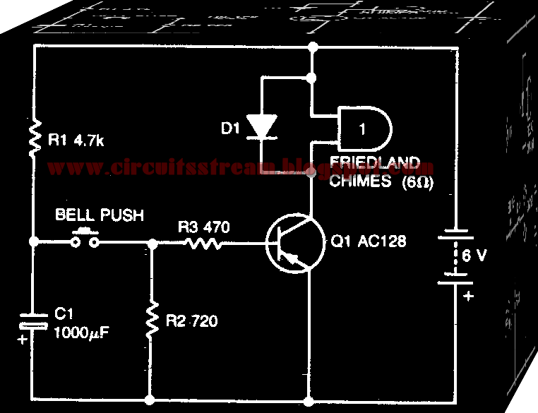
Digital Door Chimes Delay Wiring diagram Schematic
This is a simple and Digital Door Chimes Delay Circuit Diagram. This schema with values shown, this simple schema will permit one operation every 10 seconds or so. Capacitor C1 charges through Rl when the button is released Making Rl larger will increase the delay.
Digital Door Chimes Delay Circuit Diagram
Subscribe to:
Posts (Atom)