Friday, October 31, 2014

1995 Ford Ranger Wiring Diagram

1995 Ford Ranger Wiring Diagram

The Part of 1995 Ford Ranger Wiring Diagram: transmission range sensor, electronic engine control, clutch pedal position switch jumper, electronic engine control, speed control, automatic transmission, starter interupt relay, rela box, starter motor during engine starting, starter relay, manual transmission, electronic engine control, battery, starter motor solenoid, switch jumper, I/P fuse panel.
Read More..

Long Delay Stop Switch Circuit Diagram

Presettable times for train stops in stations are indispensable if you want to operate your model railway more or less realistically according to a timetable. This circuit shows how a 555 timer can be used with a relatively small timing capacitor to generate very long delay times as necessary by using a little trick (scarcely known among model railway electronic technicians): pulsed charging of the timing net-work. Such long delays can be used in hidden yards with through tracks, for instance.  As the timer is designed for half-wave operation, it requires only a single lead to the transformer and one to the switching track or reed contact when used with a Märklin AC system (H0 or H1). The other lead can be connected to any desired grounding point for the common ground of the track and lighting circuits.

Long-Delay Stop Switch Circuit diagram :

Long-Delay Stop Switch Circuit Diagram

As seen from the outside, the timer acts as a monostable flip-flop. The output (pin 3) is low in the quiescent state. If a negative signal is applied to the trigger input (pin 2), the output goes high and C4 starts charging via R3 and R4. When the voltage on C4 reaches 2/3 of the supply voltage, it discharges via an internal transistor connected to pin 7 to 1/3 of the supply voltage and the output (pin 3) goes low. The two threshold values (1/3 and 2/3) are directly proportional to the supply voltage. The duration of the output signal is independent of the supply voltage: t= 1.1(R4 + R5) × C4 

if the potentiometer is connected directly to the supply line (A and B joined). The maximum delay time that can be generated using the component values shown in the schematic diagram is 4.8 minutes. How-ever, it can be increased by a factor of approximately 10 if the timing network is charged using positive half-waves of the AC supply voltage (reduced to the 10–16-V level) instead of a constant DC voltage. 

The positive half-waves of the AC voltage reach the timing network via D2, the transistor, and D3. Diode D3 prevents C4 from being discharged between the pulses. The total resistance of R4 and R5 should not be too high (no more than 10 MΩ if possible), since electrolytic capacitors (such as are needed for C4) have significant leakage currents. Incidentally, the leakage current of aluminium electrolytic capacitors can be consider-ably reduced by using a supply voltage well below the rated voltage. Capacitor C6 is intended to suppress noise. It forms a filter network in combination with an internal voltage-divider resistor.

If a vehicle happens to remain standing over the reed switch so the magnet holds the contacts constantly closed, the timer will automatically be retriggered when the preset delay times out. In this case the relay armature will not release and the locomotive will come to the ‘end of the line’ in violation of the timetable. This problem can be reliably eliminated using R6, R7 and C5. This trigger circuit ensures that only one trigger pulse is generated, regardless of how long the reed switch remains closed. RC network R8/C7 on the reset pin ensures that the timer behaves properly on switch-on (which is far from being something to be taken for granted with many versions of the 555 or 556 dual timer).

Reed switches have several special characteristics that must be kept in mind when fitting them. The contact blades, which are made from a ferromagnetic material, assume opposite magnetic polarities under the influence of a magnetic field and attract each other. Here the position and orientation of the magnet, the distance between the magnet and the reed switch, and the direction of motion of the magnet relative to the switch are important factors. The fragility of the glass hous-ing and the thermal stress from soldering (stay at least 3 mm away from the glass housing) require a heat sink to be used between the soldering point and the glass/metal seal. A suitable tweezers or flat-jawed pliers can be used for this pur-pose. If you need to bend the leads, use flat-jawed pliers to protect the glass/metal seal against mechanical stresses. 

Matching magnets in various sizes are available from toy merchants and electronics mail-order firms. They should preferably be fitted underneath the loco-motive or carriage. However, the magnet can also be fitted on the side of a vehicle with a plastic body. In this case the reed switch can be hidden in a mast, bridge column or similar structure or placed in a tunnel, since the distance must be kept to less than around 10 mm, even with a strong magnet. If fitting the circuit still presents problems (especially with Märklin Z-gauge Mini-Club), one remedy is to generate the trigger using a unipolar digital Hall switch, such as the Siemens TLE4905L or Allegro UGN3120. To avoid coupled-in interference, the stop timer should be fitted relatively close to the Hall sensor (use screened cable if necessary). Pay attention to the polarity of the magnet when fitting it to the bottom of the vehicle. With both types of sensors, the South pole must point toward the front face of the Hall IC (the face with the type marking). The North pole is sometimes marked by a dab of paint. Generally speaking, the polarity must be determined experimentally. 

Fitting the circuit is not a problem with Z-gauge and 1-gauge tracks, since the distance between the iron parts (rails) and the Hall switch is sufficiently large. In an HO system, some modifications must be made to the track bed of the Märklin metal track. Cut a suitably sized ‘window’ between one wheel rail and the centre rail in order to prevent secondary magnetic circuits from interfering with the operation of the sensor. Keep the distance between the magnet and the case of the Hall switch between 5 and 10 mm, depending on the strength of the magnet, to ensure reliable actuation.
Read More..

Thursday, October 30, 2014

ATX Power Supply PIN OUT Connector

CPU power supply units (PSU) cede the power to the PC hardware via a numeral of cables with connectors. The generic specifications in support of various PSU form factors intended for get through with desktop systems are defined arrived Intels design guides, which are periodically revised. The hottest standard is Design conductor rev.1.2 released on February 2008. This detail combines the supplies representing ATX12V and its five variations.

For SMPS PSU surgical treatment basics envisage power supply tutorial.
Standard ATX-type power food for desktop PCs typically gain the key power connector and other 12V connectors, like well as peripheral, floppy drive, run ATA, and PCI Express® receptacles.
To support 75W PCI Express® necessities, arrived the contemporary ATX systems the old 20-pin major connector has been replaced by a 24-pin connector. Accordingly, distinct ATX-shape smps possibly will application different total of power supply wires: see the diagram in favor of pinouts of the old and new power connectors. The flag in this chart characterize recommended ensign of the wires wearing the PSU cables. The flag are publicized at this time absolutely for reference (you wont investigate them from the front). The diagrams contemplate the front (pin-border) see.

You need to look from the back of the connector to see the decorated wires. key connector uses Molex Housing Mini-Fit Jr. P/N# 39-01-2240 or else equivalent (old part quantity 5557-24R), contacts: Molex 44476-1112 or else equivalent, mating motherboard connector is Molex 44206-0007. The old 20-pin ATX connector was Molex 39-01-2200 otherwise equivalent, mating motherboard part was Molex 39-29-9202. Under some conditions new-fangled PSU can still ensue used in the field of an old PC and vise versa- distinguish our handbook on linking 20-pin PSU to 24-pin motherboard. 

To start up a halt by yourself PSU on behalf of hard purposes, you need to curt PS_ON pin to lone of the unexceptional pins. Under natural surgery, PS_ON is activated as soon as you press and statement the mainframe power button while it is fashionable maintain mode. 

All voltages are referenced to the same common (if you need to assess in the least voltage, associate the return be the forerunner of your voltmeter to any of the COM pins).

Memorandum to Apples Power Macs, basin (flanked by 1996 and 2000) and particular HP models habit proprietary (non-standard) motherboards with entirely changed pinouts.

The rated current of the core Molex connector is 6A for every pin. Which revenue with the old 20-pin comfort you cant grasp added than 18A from 3.3V and 24A from 5V. with the intention ofs why inwards premature 2000s, particular motherboards with 3.3V >18A and 5V >24A (principally dual CPU AMD systems) used an assisting 6-pin power cable. It was disinterested from ATX12V spec v2.0 in 2003 as especially pins were added to the highest connector. in place of added in sequence on form factors set eyes on our workstation PSU leader and schematics. 

SATA

While the industry began using voltage law modules (VRM) running rancid 12V2 to energize CPU and other motherboard components, the bulk of the wattage shifted to 12 volt means of transportation. as a rule of at presents motherboards supply their CPU with a separate 12 volt cable, which has 4 pins pro ATX smartness (from time to time called P4) before 8 or additional pins for EPS and non-standard climax-power systems. a quantity of PSUs may possibly gain three before four 12 volt 4-pin connectors. The part total for standard 4-pin connector is Molex 39-01-2040 before equivalent.

4-pin peripheral power connector progress to CD drives, fans, and other lesser campaign. The floppy drive connector such as the forename implies powers the floppy drive. 

Record to facilitate pin information and wire numbers clothed in run Power ATA (SATA) connector are not 1:1. at hand are three pins in support of all voltage. solitary pin from each voltage is used for pre-charge in the backplane. Mating ongoing plug of ATA campaign contains both signify and power segments.

About units could in addition arrange an elective 2x3 connector to facilitate can be situated used on behalf of additional functions, such since fan monitoring and control, IEEE-1394 power source, and a remote sensation of 3.3 vs.. 

PSU larger than 450W designed for extreme-bottom discrete graphics cards normally have further 2x3 before 2x4 connectors. They supply especially power to graphics to require extra than 75 watts whole. 
The 6-pin PCI Express® power connector is Molex part digit 0455590002.

Read More..

BD139 BD140 100W Bipolar Power Amplfier Circuit diagram

This is a plain 100 watt power amplifier designed to subsist (relatively) tranquil to build next to a reasonable fee. It has a better performance (read: musical quality) than the standard STK module amps with the intention of are used in the sphere of almost all throng advertise stereo receiver manufactured at the moment. at what time I originally built this contraption, it was since I considered necessary a 100 WPC amp and resolve not fancy slightly money. So I designed around parts I had in the supply.


The design is essentially a standard format, and I’m positively present are business entities with the purpose of are alike. To my knowlwdge, it is not an exact emulate of a commercial entity, nor am I aware of one patents on topology. on behalf of practiced builders: I am aware to many improvements and adjustments can come to pass made, but the theory was to keep it straightforward and have to achieve-able by anybody who is a circuit, and has not the patience to do a sloppy mission.

If alone crave Bipolar Transistor power amplifier circuit. , clothed in fashion HIFI OCL 100W RMS. I think this track ought to ensue an remarkable array, this circuit is the get through of the fundamental transistor BD317 and BD318 save transistor digit BD139, BD140, BC556 too comfortable in that case try to procure after the 35V power source with simply then build is not complex on behalf of other details in the same way as the answer of a only some appreciate Circuit.  Input stage is a BC556 transistor, which largely of the sincere ring benefit, and on the placid DC voltage stabilizes. This feeds a level remove stage wherever the voltage swing to (-) track references. The Transconductance stage is a Darlington, recover frerqency high-level linearity. The BD317, 318 on a instead great radio dish-heart volume is dependent on voltage. The BD319 presents this low-z and has a C (ob) of merely a hardly any of PF, which is effectively swamped by the pole-splitting 220pF cap. The commotion is supplied by BC546 in force load (current), which is approximately 20 mA. The current, until the BC556 is inadequate to approximately 70 mA taking part in the most awful belongings. 
Read More..

BD139 40 High Power Headphone Amplifier Diagram Circuit

Firstly, Id like to stress that the intended use of this circuit is only one of many possible applications. Apart from the obvious usage as a headphone amplifier, the circuit can be used for a range of applications where a wide bandwidth low power amplifier is needed. Some of the options include ...
  • Reverb drive amplifier - ideal for low and medium impedance reverb tanks
  • High current line driver - suitable for very long balanced lines
  • Low power speaker amplifier - better performance than small integrated amps
  • ... and of course, a headphone amp.
In short, the amp can be used anywhere that you need an opamp with more output current than normally available. Since most are rated for around ±20-50mA, general purpose opamps are not suitable for driving long cables or anywhere else that a relatively high output current is needed.

As a headphone amplifier, this design is very similar to others on the ESP site, but the main difference is that this one (and P70) has been built and fully tested. The design is fairly standard, and every variation was checked out before arriving at the final circuit. A photo of the prototype is shown below, and at only 64 x 38mm (2.5 x 1.5 inches) it is very small - naturally, the heatsink is not included in the dimensions.

The amplifier is capable of delivering around 1.5W into 8 ohm headphones, and 2.2W into 32 ohms - this is vastly more than will ever be needed in practice. The use of a 120 Ohm output resistor is recommended, as this is supposed to be the standard source impedance for headphones. Unfortunately, many users have found that their phones perform better when driven from a low impedance source.

HighPrototype Headphone Amplifier

The circuit is based on an opamp, with its output current boosted by a pair of transistors. Distortion is well below my measurement threshold at all levels below clipping into any impedance. Noise is virtually non-existent - even with a compression driver held to my ear, I could barely hear any, and I couldnt hear any with headphones.

WARNING
Headphones are rated in dB SPL at 1mW, and this amplifier (like many other similar headphone amps) is capable of producing extreme SPLs. The levels obtainable are sufficient to cause almost instantaneous permanent hearing damage! Never operate the amp at very high levels, and never switch the amplifier on with signal while wearing you headphones.

Always start with the volume control at minimum, and gradually increase the level until it is comfortable, but not too loud. Because of the very low distortion, it is easy to increase the level too far without noticing. Your ears are precious - safeguard them at all times.

Note the warning above - this is serious. Most headphones are capable of at least 94dB SPL at 1 mW, with some as high as 107dB SPL. Even 10mW is enough to create sound levels capable of causing hearing damage, so you must be very careful to avoid damaging levels.

Table 1 - Maximum Exposure to SPL
Note that the exposure time is for any 24 hour period, and is halved for each 3dB SPL above 85dB. The above shows the accepted standards for recommended permissible exposure time for continuous time weighted average noise, according to NIOSH (National Institute for Occupational Safety and Health) and CDC (Centers for Disease Control). Although these standards are US based, they apply pretty much equally in most countries - hearing loss does not respect national boundaries.

Description

The amplifier itself is fairly conventional, and is very similar to another shown on this site (see Project 24). This amplifier does not include the active volume control, because in general it is far easier to get a good log pot (or simply fake the pots law as described in Project 01). Likewise, it does not include the cross-feed described in Project 109. If this is desired, it is very easy to implement on a small piece of tag board, or even sky hook the few components off the bypass switch. Full details of how to do this will be included in the construction guide when PCBs are available.

The output transistors are biased using only resistors, rather than constant current sources. Extensive testing showed that using current sources made no discernible difference to performance, but increased the complexity and PCB size. Using separate caps for each biasing diode does make a difference though - and although it is relatively minor, the use of the two caps is justified IMHO.

The bias diodes should be 1N4148 or similar - power diodes are not recommended, as their forward voltage is too low. This may result in distortion around the crossover region, where one transistor turns off and the other on. As shown, crossover distortion is absolutely unmeasurable with the equipment I have available.

PrototypeFigure 1 - Headphone Amplifier Circuit Diagram

Above is the schematic of one channel. Resistors and caps use the suffix R for the right channel. The second half of the dual opamp powers the right channel. Note that the volume control shown is optional, and is not on the PCB. If needed, it may be mounted in a convenient location and the output connected to the inputs of the board as shown. D1 and D2 (L and R) are 1N4148 or similar.

One of the reasons the amp is so quiet is that the entire board runs from a regulated supply, so hum (in particular) is eliminated. Although an unregulated supply can be used, this is not recommended. The supply should be separate from that used for your preamp, because of the relatively high current drawn by the amplifier (at least with low impedance phones). A P05 preamp supply can be used, and will ensure optimum performance.

The prototype amplifier has flat frequency response from 10Hz to over 100kHz. Distortion is below my measurement threshold with any level or load impedance, and output impedance is almost immeasurably low. Your headphones may be designed to operate from a 120Ω source impedance (many are), so this may be added if it improves sound quality. Adding any series resistance will reduce the available power, but it is already far greater than you can use. Without series resistance, the minimum power into various load impedances is given below (based on ±15V supplies).

Continuous dB SPLMaximum Exposure Time
858 hours
884 hours
912 hours
941 hour
9730 minutes
10015 minutes
1037.5 minutes
106<4 minutes
109<2minutes
112~ 1 minute
115~ 30 seconds
ImpedancePower (Direct)120 Ohm Feed
8 Ohms1.5 W35 mW
32 Ohms2.2 W99 mW
65 Ohms1.1 W136 mW
120 Ohms595 mW149 mW
300 Ohms238 mW121 mW
600 Ohms119 mW82 mW
Table 2 - Output Power Vs. Impedance
This is not especially comprehensive, but will cover the majority of headphones in common use. In all cases, the available power is more than needed ... not so you can damage your hearing, but to allow adequate headroom for transients.

Construction

While it may be possible to build it using Veroboard or similar, there is a high risk that it will oscillate because of the very wide bandwidth of the amplifier. A capacitor may be added in parallel with R4 (L and R) to reduce the bandwidth if stability problems are encountered. Although I used an NE5532 opamp for the prototype, the circuit will also work with a TL072, but at reduced power. You may also substitute an OPA2134 or your favorite device, taking note of the following ...
opampThe standard pinout for a dual opamp is shown on the left. If the opamps are installed backwards, they will almost certainly fail, so be careful.

The suggested NE5532 opamp was used for the prototype, and performance is exemplary. Devices such as the TL072 will be quite satisfactory for most work, but if you prefer to use ultra low noise or wide bandwidth devices, that choice is yours.

Construction is fairly critical. Because of the wide bandwidth of the NE5532 and many other audio grade opamps, the amplifier may oscillate (the prototype initially had an oscillation at almost 500kHz), so care is needed to ensure there is adequate separation between inputs and outputs. Even a small capacitive coupling between the two may be enough to cause problems.

As shown in the photo, this amplifier needs a heatsink. While it can operate without one at low power using high impedance headphones, you need to plan for all possibilities (after all, you may purchase low impedance phones sometime in the future). The heatsink does not need to be massive, and the one shown above is fine for normal listening levels. An aluminium bracket may be used to attach to the chassis - I recommend 3mm material. Note that the heatsink should always be earthed (grounded).

The output transistors must be insulated from the heatsink. Sil-Pads™ are quite suitable because of the relatively low dissipation, but greased mica or Kapton can be used if you prefer. If you use the suggested 3mm aluminium, you can drill and tap threads into the heatsink, removing the need for nuts.

Testing

Connect to a suitable power supply - remember that the supply earth (ground) must be connected! When powering up for the first time, use 56 ohm "safety" resistors in series with each supply to limit the current in case you have made a mistake in the wiring. These will reduce the supply voltage considerably because of the bias current of the output transistors.

If the voltage at the amplifier supply pins is greater than ±6V and the output voltage is close to zero, then the amplifier is probably working fine. If you have an oscilloscope, check for oscillation at the outputs ... at all volume control settings. Do this without connecting your headphones - if the amp oscillates, it may damage them.

Once you are sure that all is well, you may remove the safety resistors and permanently wire the amplifier into your chassis.
source: http://sound.westhost.com/project113.htm
Read More..

Modem Off Indicator Circuit Diagram

The modem off indicator is intended especially for serious Internet surfers. It will be seen that the circuit of the indicator cannot be much simpler, or there might be nothing left. In spite of its simplicity, it may prove to be a cost-saving device, since it shows at a glance whether the telephone line is free again after the modem has been used. This obviates high telephone charges in case for some reason the modem continues to operate. The circuit depends on the fact that there is a potential of about 40 V on the telephone line when it is not busy. This voltage drops sharply when a telephone call is being made. If, therefore, the circuit is linked to telephone terminals a and b, the lighting of the green LED shows that the line is not busy in error.

Modem Off Indicator Circuit diagram:


 Modem Off Indicator Circuit Diagram

The bridge rectifier ensures that the polarity of the line voltage is of no consequence. This has the additional benefit that polarity protection for the LED is not necessary. To make sure that the telephone line is not loaded unnecessarily, the LED is a high efficiency type. This type lights at a current as low as 2 mA, and this is, therefore the current arranged through it by resistor R1.

WARNING.
In spite of the liberal age we live in, it is highly probable that in many countries it is not allowed to connect the indicator across the telephone lines. Seek advice of your local telephone company that owns or operates the telephone network.
Read More..

Balanced Microphone Amplifier Diagram Circuit

We published a design for a stereo microphone preamplifier with balanced inputs and a phantom power supply. The heart of this circuit was a special Analog Devices IC, the SSM2017. Unfortunately, this IC has been discontinued. In its place, the company recommends using the pin-compatible AMP02 from its current product line. However, and again unfortunately, the specifications of this opamp make it considerably less suitable for use as a microphone amplifier. By contrast, Texas Instruments (in their Burr Brown product line) offer an integrated instrumentation amplifier (type 1NA217) that has better specifications for this purpose.


Incidentally, this IC is also recommended as a replacement for the SSM2017. It features internal current feedback, which ensures low distortion (THD + noise is 0.004 % at a gain of 100), low input-stage noise (1.3 nV/√Hz) and wide bandwidth (800 kHz at a gain of 100). The supply voltage range is ±4.5 V to ±18 V. The maximum current consumption of the 1NA217 is ±12 mA. The gain is determined by only one resistance, which is the resistance between pins 1 and 8 of the IC. The circuit shown here is a standard application circuit for this instrumentation amplifier. R1 and R2 provide a separate phantom supply for the microphone connected to the amplifier (this is primarily used with professional equipment).

Balanced
Balanced Microphone Amplifier Circuit Diagram

This supply can be enabled or disabled using S1. C1 and C2 prevent the phantom voltage from appearing at the inputs of the amplifier. If a phantom supply is not used, R1 and R2 can be omitted, and it is then better to use MKT types for C1 and C2. Diodes D1–D4 are included to protect the inputs of the 1NA217 against high input voltages (such as may occur when the phantom supply is switched on). R4 and R5 hold the bias voltage of the input stage at ground potential. The gain is made variable by including potentiometer P1 in series with R6. A special reverse log-taper audio potentiometer is recommended for P1 to allow the volume adjustment to follow a linear dB scale.

The input bias currents (12 µA maximum!) produce an offset voltage across the input resistors (R4 and R5). Depending on the gain, this can lead to a rather large offset voltage at the output (several volts). If you want to avoid using a decoupling capacitor at the output, an active offset compensation circuit provides a solution. In this circuit, a FET-input opamp with a low input offset (an OPA137) is used for this purpose. It acts as an integrator that provides reverse feedback to pin 5, so the DC output level is always held to 0 V. This opamp is not in the audio signal path, so it does not affect signal quality. Naturally, other types of low-offset opamps could also be used for this purpose. The current consumption of the circuit is primarily determined by the quiescent current of IC1, since the OPA137 consumes only 0.22 mA.
Author: T. Giesberts
Copyright: Elektor Electronics
Read More..

Wednesday, October 29, 2014

Diagram LM 3915 Sound Level Meter Circuit

LMThis is a one chip sound level meter that can be use for displaying sound level of an amplifier or simply the sound level from a microphone.The heart of the circuit is IC LM 3915 Audio level IC.Even though it is a stand alone IC , a peak detector based on Transistor BC 558 and diode 1N4001 is also included for better performance.

Supply voltage can be from 3V to 20V.The input is set for audio line voltage (1V peak to peak) and has a max input voltage of 1.3V. To make the circuit use a moving dot display instead of bar graph display,Pin 9 can be should be disconnected from +V.

Part List

C1 2.2uF 25V Electrolytic Capacitor
C2, C3 0.1uF Ceramic Disc Capacitor
R1, R3 1K 1/4W Resistor
R2 10K 1/4W Resistor
R4 100K 1/4W Resistor
R5 1M 1/4W Resistor
D1 1N4001 Silicon Diode
Q1 BC 558 PNP Transistor
LED1-LED10 Standard LED or LED Array
U1 LM3915 Audio Level IC
MISC Board, Wire, Socket For U1
Read More..

Watch R LG G is presented The watch with round screen looks great

Watch
 
Did not have to wait long. LG introduces its new smart watch with round screen and Android Wear, Watch the LG G R.

The new LG smart watch has a 1.3 inch OLED screen, completely circular. LG said that the LG G Watch R is not trying to replace the current G Watch, it is offering an alternative. In a way, the LG G Watch R is more elegant and feels more like a traditional clock. This is a good ad, especially the Moto 360 should be officially announced next week.

In fact, the design of the LG G Watch R looks much better than the original and improves some of its components.

To begin, the screen has a better resolution (320 x 320 vs. 280 x 280), a battery of 410mAh (vs. 400mAh). Additionally, the R G Watch features a heart rate monitor and a button on the late real part.

Other features of the LG G Watch R 400 include a Snapdragon 1.2Ghz processor, 4GB of internal storage, 512MB of RAM, will only in black color and is waterproof.

The LG G Watch goes on sale in October, but the company has not announced a price, which varies only in each market.

Clearly, the LG G Watch R has excellent design and looks very similar to a traditional clock. Foul see how it looks in real life, but this kind of watches are the ones who can really help this category of smart watches finally take off.
Read More..

Nmos Power Amplifier Series Part 1

Nmos200 - TO220
A compact power amplifier module capable of up to 200 watts into a 4 ohm load depending on power supply and the output mosfets used.  The module is limited to rails of +/- 50v max.  The amplifier can be built using either TO220 or TO247 style Mosfets.

Schematic Diagram Nmos200-TO220


Layout Nmos200-TO220


Nmos200 - TO247
 Nmos200 - TO247 Stereo


Schematic Diagram Nmos200-TO247

Layout Nmos200-TO247

Read More..

Circuit Diagram of Remote Control Tester

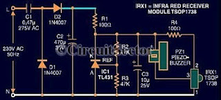
Here is an infrared remote control tester circuit that can be made without spenting much money.This IR tester build around an infrared reciever module TSOP1738. We can observe the remote control state by listening to the buzzer sound. The circuit is very sensitive and it support a range of about 5 meters.

The infrared receiver module normally remains high and the piezo buzzer is in silent mode. When the IR module receives a signal from the remote control,Its output goes low and the piezo buzzer sounds.

Circuit

Notes
  • Assemble the circuit on a Common PCB and enclose in a small box.
  • Make sure the IR receiver made visible outside.
  • You can directly plug the circuit into mains
Read More..

Tuesday, October 28, 2014

Two Way Active Crossover

2 Way Active Crossover alive Cantankerous completed is adequately beeline cheeky. It consists of a absorber and two 3rd order, 18 dB for every octave filters. single low canyon and the added from head to foot. The cantankerous ended profusion is firm on 2Khz and is advised representing AEK’s 400watt apiece access supporter/grand piano Amp systems. perceptibly on your own lone access is deceptive at this time.

Two Way Active Crossover

The belt akin audio arresting enters the absorber area it is backward available of time. This is to atone representing the filters which desire change the advent afresh appropriately abiding the arresting to it’s able period. The filters are additional-otherwise-not as much of customary low and aerial canyon filters appropriately however, added capacitors and resistors endure been added trendy adjustment to follow the selflessness bottomward to a bare minimum appliance by yourself E12 components.

This ambit may perhaps not transpire of awfully abundant make use of to someone for example it was accurately advised to clothing the applications. It is not variable or else switchable used for two reasons. initially, it didn’t charge to be back the backdrop of the apostle array were already acknowledged. And secondly, the added complication was deposit into the correctness of the crossover more accurately than it’s flexibility. The filters are akin stylish story to anniversary added being able-bodied as can be alive established appliance lonesome E12 components. If switching were to be lively to agreement a ambit of profusion options, a accommodation would agree to to be fictitious on spell out accuracy.

The abandoned added way to accomplish a time-honored crossover architecture and advance precision would apparently subsist to management Switched capacitor shed light on architecture blocks. in the sphere of theory, two 18or 24dB for every octave filters may well be complete such to facilitate they tracked anniversary added by certainty bound to the aforementioned control. This would live a fussy agreement but I haven’t had the befalling to attest this tools pro this affectionate of hard work. My primary thing was the breach through of switching babble appliance such a design.

Therefore this architecture represents the simplest access I possibly will booty and still make the adapted outcome.
Read More..

Circuit diagram BA1404 based Stereo transmitter

Using BA1404 can be designed a very simple and useful stereo fm stereo modulator electronic project . This BA1404 fm stereo modulator device works in FM broadcast band ( 75- 108MHz) and require few external common components .
The BA1404 fm stereo modulator Ic contains all parts needed to design an simple high efficiency stereo transmitter circuit , it contains a stereo modulator that creates stereo composites signals ,an FM modulator that creates FM signals and a RF amplifier .

The fm stereo transmitter develops composite signals made up of a main(L+R) signal and sub(L-R) signal and a pilot (19KHz) signal using a 38KHz crystal oscillators.
The RF amplifier transmits the stereo encoded signals and is also a buffer for FM modulator .
For this FM stereo transmitter circuit you’ll need a DC power supply that can provide an output voltage between 1.5 an 3 volts . This fm stereo transmitter circuit project can be used for FM stereo transmitters or wireless microphone circuits .
The L1 coil must have 3 turns of 0.5mm wire on a 5 mm core .
Antenna used in this transmitter can be an common telescopic antenna or a 60-80 mm long Cu wire .
Read More..

Polk Audio 100W Subwoofer

The PSW10 subwoofer fills indoors the foundation outcome of your institution acting usage, so your foremost speakers dont hold to put on deep duty, as an alternative having solitary to procreate the normal and climax frequencies. If youa propos looking pro your original subwoofer, look rejection extra than the PSW10. Its a horrible solution for completing your sound approach and spirit take your viewing experience, movies, games and tube to a top level of enjoyment.

Polk

Dynamic Balance® Woofer Design. Polk perfected the method of analyzing a presenters minuscule behavior with laser Interferometry. With with the aim of in sequence during offer, Polk engineers limited the ideal combination of resources, geometry and construction techniques to factually “song unconscious” superfluous resonance. The product is a subwoofer with the intention of delivers innocent, distortion uncontrolled deep low.

Klippel Optimized Woofer. Using a state-of-the-drawing Klippel Distortion Analyzer, Polk engineers optimized the woofers motor form, voice coil alignment and suspension, bringing you the preeminent on the cards performance even next to the generally extreme listening levels.

Composite Polymer funnel We dont expenditure reduced paper cardboard woofers. This is the real deal and part of why the PSW 10 subwoofer outperforms the competition.

Read More..

Monday, October 27, 2014

3 Volt Operated Power Amplifier Circuits

This is an audio amplifier with the purpose of can live used with a minor 3 volt Battery Operated,Current get through having the status of not much as 5 milliamps.And amplification up to 500 mW.

3 Volt Operated Power Amplifier Circuit Diagram
Which is sufficient to swell the sound from a sound a propos otherwise the disc totter work comatose to the minor speakers obviously. 3 whilst entering the power supply 3-volt circuit IC1 numeral LM386 amplifier IC size is 300-800 mW, Depending on the power supply circuit with,This is from 3-15 volts. just the once entered into the input pin 3,The non inverting pin to amplifier non-return segment.C1 self-control ensue served slice out the blare input to ground.And C2 increases the rate of amplifier,C2 is to add extra denomination.But if the C2 Too much distortion (the C2 be supposed to not exceed 100uF).The output of IC1 is comatose of the pin 5 through C4 coupling audio signals to better and DC frustrate and not voted for to the narrator.on behalf of the audio portion desire in addition be present fed back through R2 and C3 to the extraordinary frequency response better.
Read More..

TA8210AH 2 x 22W BTL Car Amplifier Circuit

This is a circuit of 2 x 22 watt BTL amplifier using IC TA8210AH. It is not only an auto amplifier, ideal for a low-frequency auditory approach those hi-fi, with a very good linear feature. Can be fueled by a 12 volt car battery but shi from a 12 volt charger. The chip incorporates four bridge amplifiers available in two by two in order to ensure the output 22 watts per channel on 4 ohms.
TA8210AHTA8210AH - 2 x 22W BTL Car Power Amplifier Circuit

Note:
  • IC TA8210AH must be connected to a heat sink. A computer cabinet fan can also be used in addition.
  • The circuit roughly draws 6A current at 18 V at full volume.So the power supply must be any thing more than 6A.
Absolute Maximum Ratings of IC TA8210AH
  • Peak supply voltage (0.2s): 50 V
  • supply voltage VCC (DC): 25 V
  • Operating supply voltage VCC (opr): 18 V
  • Output current (peak): 9 A
  • Power dissipation PD: 50 W
  • Operating temperature: 30~85 °C
  • Storage temperature: 55~150 °C
List Componet
C1,C2 : 4,7uF/35V
C3,C7 : 47uF/35V
C4 : 220uF/35
C5,C6 : 1nF
C8,C10,C11,C12 : 0,1uF/35V
C9 : 2200uf/35V
IC : TA8210AH/AL
HL1 : LED
R1 : 2 k
R2,R2,R3,R4,R5 : 2,2 Ohm
Read More..

SAMSUNG protect circuit with LA76931

Following is the protect circuit Samsung TV which use IC LA76931 as basic working the protect circuit. This Protect Circuit LA76891 located at pin-30 whichconnected to the collector of transistor Q902.In normal conditions the voltage at the base of Q902 is "low" and the voltage at pin-30 is "high". For the temporary crippling protect, it can be removed Q902 (or to the emitter-base short).

SAMSUNG protect circuit with LA76931
Sampling circuit protect from:

Vertical Protect. Pulses of the vertical-out rectified by diode D355, so that the base voltage is approximately 0.6V Q904 ,and collector voltage is 0v.
X-ray Protect (option). Sampled using a heater voltage of the circuit as shown below. Normal vltage in x-ray path to the base of Q902 is zero.

ABL protect. If there is damage to flyback voltage which can cause a high rise ABL, then protect circuit will actively work.
Read More..

Sunday, October 26, 2014

Digital visitor counter

Digital visitor counter is a reliable circuit that takes over the task of counting Number of Persons/ Visitors in the Room very Accurately. When somebody enters into the Room then the Counter is Incremented by one and when any one leaves the room then the Counter is Decremented by One. The total number of Persons inside the Room is displayed on the seven segment displays. The microcontroller do the above job it receives the signals from the sensors, and this signals operated under the control of software which is stored in ROM.

Digital visitor counter

Read More..

IC 74160 HZ not pass filter


In sometimes when want to decrease especial frequency noise that want only. This circuit can help you , it does will not let 60HZ frequencies s can change. Then decrease the noise. By use the integrated circuit , 741 numbers highly popular , economize and don’t seek buy easy with , if , friends , want to filter especial which frequency the one frequency. As a result change the value RC see the detail has added in the circuit sir.
Read More..

Saturday, October 25, 2014

Audio phase shift oscillator Circuit Diagram

Here is a phase-shift audio oscillator with excellent distortion characteristics thanks to “softened” diode limiting provided by the 1N914 and resistor divider and degenerated gain provided by the 68 ohm emitter resistor. For minimum distortion, increase the 68 ohm resistor to a point just below where oscillation stops. A simple buffer may be added for driving lower impedance loads.


The output amplitude will be about 5 volts p-p but one of the 1N914’s 10k divider resistors may be changed for a different output amplitude. The circuit will work well with a power supply voltage other than 9 volts but the 68 ohm resistor may need adjustment
Read More..

Friday, October 24, 2014

AT89C2051 microcontroller circuit

Real time controller is a device used to exercise control over household device continuously ongoing and scheduled. The series of Real Time Controllers with microcontroller AT89C2051 which dituls in this article is a tool that can do that serve targeted. The series of Real Time Controller with Microcontroller AT89C2051 Atmel AT89C2051 uses a data processor and controller as device installed.
In the application directly devices requires a separate interface from a wide range of Real Time Controllers with this AT89C2051 microcontroller. When will connect the device with the AC power source to use interface optocoupler (MOC) or solid state relay. Devices that can be connected with the series of Real Time Controller with Microcontroller AT89C2051 include lights, water machines, fans, electronic gate. The series of Real Time Controllers with this AT89C2051 microcontroller to control a height of water level, controlling the flame lights the scheduled SCARA and censored.

Specifications Series Real Time Controller with AT89C2051 Microcontroller
The series of Real Time Controller with Microcontroller AT89C2051 uses a computer to perform serial communication settings via computer. The series of Real Time Controller with Microcontroller AT89C2051 has 6 units of output channels that can be independently controlled depending on the program induced in the tool. Output in the series of Real Time Controller with AT89C2051 microcontroller requires an interface to deal with equipment that will be in control.
Read More..

Thursday, October 23, 2014

Automatic Battery Charger Circuit

Basically the circuit designed above have a very simple way of working, where the circuit is designed so that does not happen short circuit or short circuit between the voltage supply with batteries that will be in-charge.


Automatic

 It is true that if any one wants to try to direct mengghubungkan between supply with batteries then the batteries can be sure will be filled. But the current flowing through a charged battery can not be controlled and if the battery is full, the batteries will be damaged or worn out if it remains on the short circuit condition.

Working Principle Battery Charger

By the time we put an empty battery charging terminals, transistor Q1 will be activated immediately because the current flows through R1 and would trigger a transistor Q1 base. In this condition the flow that would fill the batteries mostly comes from the collector of Q1 is connected directly to the positive terminal of supply. Then during the charging process increases the battery voltage will increase the current flowing in Q2 base via 10 Kohm R5, VR1 and diode D2. VR1 is a component that is used as an initial calibration to determine the exact position in the planning process of switching circuit. For VR1 you can use a trimpot or potensio according to your taste. At the beginning of filling, arrange potensio at position D3 LED indicators on the condition of death, and the current flowing into the collector of Q1 is not too big and not too small.

If the battery is fully charged, the LED indicator will light up automatically because of an increase in voltage on the battery charge will cause the increase of current flowing at the base of transistor Q2 and will terminate the charging cycle due to transistor Q1 having a cut-off due to lack of base current. Why on condition Q1 base current will experience a shortage of this is because almost all the current flowing in R1 10 Kohm will switch to a diode D1 which is logically connected directly with ground experience due Q2 saturated.
.
Component List
1. Resistors: R1 (10 Kohm), R2 (680 ohms), R3 (100 Kohm), R5 (10 Kohm) and VR1 (Potensio / trimpot = 100 Kohm)
2. Diodes: D1 & D2 (IN4002) and D3 (Led)
3. Transistors: Q1 and Q2 (2N3904)
4. 9 volt power supply
Read More..

200 Watt Stereo Car Amplifier

IC TA8210AH By using this you can apply a series of audio power amplifier is the car audio system. In general, all the speakers in the car using a subwoofer speaker, and woofer. Because the car is not big room so the sound is being required is not too high.

Audio amplifier circuit can work at a minimum voltage 12-volt DC, if supplied under voltage 12-volt amplifier work will be less than the maximum. This amplifier output power up to 200W or 2 x 100W stereo with 8 ohm impedance.


Part List :


Resistor

R1 =1K

R2 =50K trim

R3 =1K

R4 =50K trim

R5 =680R

R6 =680R

R7 =150K

R8 =2R2

R9 =2R2

R10=2R2

R11=2R2


Capacitor

C1 =1uF

C2 =1uF

C3 =47uF

C4 =47uF

C5 =100n/400V

C6 =220uF

C7 =220uF

C8 =100n/400V

C9 =100n/400V

C10=100n/400V


Intregated Circuit

IC1=TA8210AH


Connector

X2-3=in R

X2-2=gnd

X2-1=in L

X1-1,X1-2=Out R

X1-3,X1-4=Out L
Read More..

Micropower Voltage Regulator

This circuit was industrial to power an AVR microcontroller from a 12 opposed to run-acid battery. The watchdog itself draws solitary 14 µA. Of avenue, at hand are dyed-in-the-wool ICs, in lieu of model from Linear machinery or else Maxim, which can subsist used, but these can be very brutally to pick up grasp of and are commonly barely to be had during SMD letters these days. These difficulties are simply and quickly avoided using this discrete circuit. The succession control device factor is the widely-presented type BS170 FET. whilst power is useful it is driven on via R1. When the output voltage reaches 5.1 opposed to, T2 starts to conduct and limits some advance gradient stylish the output voltage by pulling down the voltage on the gate of T1. The output voltage can be present calculated seeing that follows:

Micropower Voltage Regulator Circuit Schematic


OUT = (VLED + VBE) × (R4 + R2) / R4

Anywhere we can agreed ULED by 1.6 in opposition to and UBE at 0.5 V. The warmth coefficients of ULED and UBE can moreover be incorporated into the formula. The circuit is so effortless with the intention of of line someone has thinking of it ahead of. The author’s hard work control bowed up an illustration appearing in a collection of reference circuits dating from 1967: the example is very alike to this circuit, although it used germanium transistors and of choice here was refusal FET. The voltage reference was a Zener diode, and the circuit was designed used for currents of up to 10 A. Perhaps our readers pray be there able to unearth even earlier examples of two-transistor regulators using this belief?
Read More..

Subwoofer Pre Amp Filter

Acoustic spectrum is extended by the 20Hz frequency is very low and reaches as high frequency 20000Hz. In the low frequency is lowered sense of direction. This reasoning leads us to attribute to the speakers use of very low frequency. Making it to you we propose to distinguish these frequencies, in order for him to lead us on a suitable amplifier.
Acoustic filter are met at different points in the sound system. Applications knownest they are filter baxandal to organize low-and high-frequency tones and crossover filter where the acoustics are separated in the subareas, for it leads to the appropriate speakers. Applications that you can we propose is a simple filter that limits the acoustic region (20-20000Hz) in 20-100Hz region.

With manufacturing, we propose that you can you can make an active filter for you lead a very low frequency loudspeaker. With this you will put a big one between speaker HIFI speakers from you. In order for you to have a complete picture of sound you will need also an appropriate amplifier. In the entry of circuit you will connect the two roads out of the preamplifier or the exit of the preamplifier few.

The series production in order to allocate out of the facility led a series of subwoofer power. If for some reason you do not have space for you to put the third speaker in the courtroom, then you can choose a smaller speaker. This output will depend on the type of music that you hear. If in deed you have the space, then after you create a filter and still say thank you, you can he recommend your friends or still makes each other to your friends.
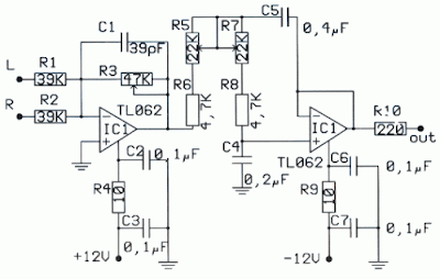
Circuit diagram

Filter
Filter | PreAmp Subwoofer circuit diagram


Parts

R1 = 39 Kohm , R2 = 39 Kohm,R3 = 47 Kohm,R4 = 10 Ohm,R5 = 22 Kohm,R6 = 4.7 Kohm,R7 = 22 Kohm, R8 = 4.7 Kohm, R9 = 10 Ohm, R10 = 220 Ohm, C1 = 39 pF,C2 = 0.1 UF,C3 = 0.1 UF, C4 = 0.2 UF, C5 = 0.4 UF, C6 = 0.1, UF C7 = 0.1 UF, IC1 = TL064

In the form that appears theoretical filter circuit. At first glance we see three different circuits which are mainly produced by two rounds of operational amplifiers. This circuit is a mixture, with the assistance variable amplifier and variable filters. Late-making requires a series of operations catering catering with the same trend with  ± 12. operational amplifier which is the active element for this circuit is the type of dual operation as a TL082 and NE5532

The operational amplifier is included in a family is equipped with field-effect transistor IFET in their entries. Each member is allocated a family in bipolar transistor circuits and field effect. This circuit can function in a high inclination, because of their high propensity to use transistors. Also they have the high honor rhythm elevation (slew rate), low polarization at this time for entry and little influenced by temperature. The operational amplifier has an area of 3MHz unity gain bandwidth. Another important element for them is a great choice reject noise, there are currently in the line of catering.

Price refused to greater than 80dB, their consumption is small, from 11 to 3 mA. They briefly sold internally with eight pins and allocate two operational amplifiers, In the same row 14 pin in short they combine four operations, the trade them for sale with code TL074, TL084 and TL064, a nutshell with eight pins they sold the operational amplifier TL071 TL061 kajTL081 . In manufacturing we use the TL082 that has two operational. First operation of TL082 he worked as an amplifier and mixed with two channels, the entry is negative, it is a little mixed with the two resistances. A potentiometer on the steps of determining the aid circuit. At this point the left wing and right-channel preamplifier they added means of two resistances. En operational continuity with the help strengthen the signal is made depending on the price that has been potentiometer.

Filter
PCB layout

Place runner comparable with the assistance of the circuit. The second operational amplifier is a filter manufacturing. Filters from the acoustic frequency from second grade and he made a round of operational amplifiers. This filter section with variable frequency low-cut. This frequency can be changed and took the price of very low frequency of 30Hz or still exceeds 150Hz. The frequency of the filter depends on the price cuts that have circuit elements. Change the value of the elements that we can have a frequency cut 150Iz, 130Hz, 100Hz, 7A? Z, 6A? Z even 3A? Z, is the price that they can be achieved by simple rotation of the double potentiometer. Filter circuit has been made about an operation that has completed a TL082 dual operational amplifier. In the filter out we will connect the plug load which is connected amplifier. In a series of exit are presented, which are limited as to the extent of frequency, the signal applied in the entry of the circuit.
Read More..

Wednesday, October 22, 2014

Surround Power Amplifier LM3886

Audio Power Amplifier is an important part in the reproduction of sound in a sound system. Audio Power Amplifier LM 3886 with power IC Audio Power Amplifier is a highly capable and able to produce 68 Watts with power rata2 4Ohm load and capable of producing power 38 Watt with 8Ohm load. 
With good sound reproduction capabilities of 20Hz-20kHz is also included on this LM3886 Audio Power Amplifier. LM3886 Audio Power Amplifier is equipped with spike protection that will protect the output circuit from overvoltage, undervoltage, overloads, konrsleting power supply, thermal runawaydan peak temperature. Audio Power Amplifier LM3886 also features a noise reduction system which can keep the audio from the noise well.

Basic Audio Power Amplifier Series LM3886 


Audio Power Amplifier LM3886 

Feature owned LM3886 Audio Power Amplifier 

68W cont. avg. output power into 4Ω at VCC = ± 28V
38W cont. avg. output power into 8Ω at VCC = ± 28V
50W cont. avg. output power into 8Ω at VCC = ± 35V
135W instantaneous peak output power capability
Signal-to-Noise Ratio ≥ 92dB
An input mute function
Output protection from a short to ground or to the supplies via internal current limiting circuitry
Output over-voltage protection against transients from inductive loads
Supply under-voltage protection, not allowing internal biasing to occur Pls | VEE | + | VCC | ≤ 12V, Thus eliminating turn-on and turn-off transients
11-lead TO-220 package
Wide supply range 20V - 94V
Application of Audio Power Amplifier LM3886
Stereo audio system
Active Speaker
High End Audio Power TV
Suround Power Amplifier
Read More..

Sunday, October 19, 2014

0 50V 1A Laboratory Power Supply Variable Voltage


Laboratory Power Supply – Variable voltage from 0V to 50V and variable current from 0A to 1A
Reverse engineered circuit diagram of an expensive commercial variable lab power supply. This unit is designed around an ordinary op-amp and easy to obtain parts. Although the unit uses a single transformer with two output windings the circuit works equally well using a big transformer and a little transformer.

Read More Source:http://members.shaw.ca/novotill/LabSupply50V1A/index.htm
Thank you.
Read More..

Saturday, October 18, 2014

Motor Bike Headlight Controller Circuit Diagram

This circuit automatically turns a motor cycles headlight on and off, independently of both the light and ignition switches, provided the battery is fully charged. The first stage uses the 22O resistor and ZD1 to hold transistor Q1 off while the motor is not running; it draws about 2mA. Once the battery voltage exceeds 7.0V during charging, Q1 begins to turn on.

The last stage uses the 22O resistor and ZD2 to turn on transistor Q2, which pulls the base of Q1 down, switching it hard on. In conjunction with the Vbe drop of Q2, ZD2 will turn off Q2 at a battery voltage of about 6.7V. In practice, this means that the headlight will be on most of the time while the motor is running and charging the battery. Heatsinks are required for both transistors. The circuit can be mounted adjacent to the battery with a single lead going to the headlight power feed.

Circuit diagram:
 motor bike headlight controller schematic circuit diagram
Motor Bike Headlight Controller Circuit Diagram
Parts:

P1 = 5R - 3W
R1 = 220R -1W
R2 = 1R - 1W
R3 = 22R - 5W
R4 = 22R - 5W
Q1 = BD139
Q2 = MJ4502
D1 = 6.2V - 1WZener
D2 = 6.2V - 1WZener
B1 = 6.6V - 7.2V
F1 = Fuse 15A
LP1 = DIP Beam 6V-25W Halogen
Read More..

Automatic Headlight Reminder circuit and explanation

Do you drive an older car without an automatic "lights-on" warning circuit? If so, youve probably accidentally left the lights on and flattened the battery on one or more occasions. This headlights reminder circuit will prevent that. Its more complicated than other circuits but its also more versatile. As shown, the circuit uses two low-cost ICs. IC1 is a 555 timer which is wired to operate in astable mode. Its output clocks IC2, a 4017B decade counter. IC2 in turn drives a row of indicator LEDs and also resets IC1 (after about 10s) via transistor Q2.

The circuit works like this:

when the ignition is on, transistor Q1 is also on and this pulls pin 4 of IC1 low. As a result, IC1 is held reset and no clock pulses are fed to IC2. Conversely, if the ignition is turned off, Q1 will turn off and so IC1 will start oscillating and sound the piezo siren. At the same time, IC1 will clock IC2 and so LEDs 1-10 will light in sequence and stop (after about 10s) with the last LED (LED10) remaining on. Thats because, when IC2s O9 output (ie, pin 11) goes high, Q2 also turns on and this pulls pin 4 of IC1 low, thus stopping the oscillator (and the siren).

Circuit diagram:
Automatic Headlight Reminder Circuit Diagram
Note:

That different colored LEDs are used to make the display look eye-catching but you make all LEDs the same color if you wish. Installing optional diode D1 will alter IC1s frequency and this will alter the display rate. Finally, if the lights are turned off and then back on again, the alarm will automatically retrigger. LED1 is always on if the lights are turned on. If you dont want the LED display, just leave the LEDs out.

Author: L. Marshall - Copyright: Silicon Chip Electronics
Read More..

1 5v to 9v INVERTER

This very clever circuit will convert 1.5v to 9v to take the place of those expensive 9v batteries. But the clever part is the voltage regulating section. It reduces the current to less than 10mA when no current is being drawn from the output. You can use two or three old cells for the supply and the circuit will totally use up all the energy from the cells. Its a great circuit for using up those old cells. With a 470R load, the output current is 20mA and the voltage drop is less than 10mV. It is best to use 3 old cells as this will deliver about 2.5v to 3v and the circuit will produce an efficiency of about 70%. Adjust the 15k resistor for 9v.

source : http://www.talkingelectronics.com.au/projects/200TrCcts/200TrCcts.html
Read More..

LIE DETECTOR Diagram

LIE DETECTOR
This circuit detects the resistance between your fingers to produce an oscillation. The detection-points will detect resistances as high as 300k and as the resistance decreases, the frequency increases.


Separate the two touch pads and attach them to the back of each hand. As the subject feels nervous, he will sweat and change the frequency of the circuit.
The photos show the circuit built on PC boards with separate touch pads.
 
source : http://www.talkingelectronics.com.au/projects/200TrCcts/200TrCcts.html
Read More..

Friday, October 17, 2014

30 Watt Audio Power Amplifier Schematic

Including Preamp, Tone Controls, Reg dc Power Supply, 18 Watt into 8 Ohm - 30W into 4 Ohm loads


This project was a sort of challenge: designing an audio amplifier capable of delivering a decent output power with a minimum parts count, without sacrificing quality. The Power Amplifier section employs only three transistors and a handful of resistors and capacitors in a shunt feedback configuration but can deliver more than 18W into 8 Ohm with 0.08% THD @ 1KHz at the onset of clipping (0.04% @ 1W - 1KHz and 0.02% @ 1W - 10KHz) and up to 30W into a 4 Ohm load.

To obtain such a performance and to ensure overall stability of this very simple circuitry, a suitable regulated dc power supply is mandatory. This is not a snag because it also helps in keeping noise and hum of the preamp to very low levels and guarantees a predictable output power into different load impedance. Finally, as the amplifier requires only a single rail supply, a very good dc voltage regulator capable of supplying more than 2 Amps @ 40V can be implemented with a few parts also.


Circuit diagram:
 30 watt mosfet audio power amplifier schematic circuit diagram
Audio Power Amplifier Circuit Diagram


Power Amplifier Parts:

R1 = 2K2 1/4W Resistor
R2 = 27K 1/4W Resistor
R3 = 2K2 1/2W Trimmers Cermet
R4 = 2K2 1/2W Trimmers Cermet
R5 = 100R 1/4W Resistor
R6 = 1K 1/4W Resistor
R7 = 330R 1/4W Resistors
R8 = 330R 1/4W Resistors

C1 = 22µF 25V Electrolytic Capacitor
C2 = 47pF 63V Polystyrene or Ceramic Capacitor
C3 = 100µF 50V Electrolytic Capacitors
C4 = 100µF 50V Electrolytic Capacitors
C5 = 2200µF 50V Electrolytic Capacitor

Q1 = BC550C 45V 100mA Low noise High gain NPN Transistor
Q2 = IRF530 100V 14A N-Channel Hexfet Transistor (or MTP12N10)
Q3 = IRF9530 100V 12A P-Channel Hexfet Transistor (or MTP12P10)


Setting up the Power Amplifier:
  1. The setup of this amplifier must be done carefully and with no haste:
  2. Connect the Power Supply Unit (previously tested separately) to the Power Amplifier but not the Preamp: the input of the Power Amplifier must be left open.
  3. Rotate the cursor of R4 fully towards Q1 Collector.
  4. Set the cursor of R3 to about the middle of its travel.
  5. Connect a suitable loudspeaker or a 8 Ohm 20W resistor to the amplifier output.
  6. Connect a Multimeter, set to measure about 50V fsd, across the positive end of C5 and the negative ground.
  7. Switch on the supply and rotate R3 very slowly in order to read about 23V on the Multimeter display.
  8. Switch off the supply, disconnect the Multimeter and reconnect it, set to measure at least 1Amp fsd, in series to the positive supply (the possible use of a second Multimeter in this place will be very welcomed).
  9. Switch on the supply and rotate R4 very slowly until a reading of about 120mA is displayed.
  10. Check again the voltage at the positive end of C5 and readjust R3 if necessary.
  11. If R3 was readjusted, R4 will surely require some readjustment.
  12. Wait about 15 minutes, watch if the current is varying and readjust if necessary.
  13. Please note that R3 and R4 are very sensitive: very small movements will cause rather high voltage or current variations, so be careful.
  14. Those lucky enough to reach an oscilloscope and a 1KHz sine wave generator, can drive the amplifier to the maximum output power and adjust R3 in order to obtain a symmetrical clipping of the sine wave displayed.


Preamplifier Section:


The Preamp sensitivity and overload margin were designed to cope with most modern music program sources like CD players, Tape recorders, iPods, Computer audio outputs, Tuners etc. The source selecting switches and input connectors are not shown and their number and arrangement are left to the constructors choice. To obtain a very high input overload margin, the volume control was placed at the preamp input.

After a unity gain, impedance converter stage (Q1) a negative-feedback Baxandall-type Bass and Treble tone control stage was added. As this stage must provide some gain (about 5.6 times) a very low noise, "bootstrapped" two-transistors circuitry with FET-input was implemented. This stage features also excellent THD figures up to 4V RMS output and a low output impedance, necessary to drive properly the Mini-MosFet Power Amplifier, but can also be used for other purposes.


Circuit diagram:
 tone controller and preamplifier circuit diagram for 30 watt mosfet audio power amplifier schematic
Preamplifier Circuit Diagram For Power Amplifier


Preamplifier Parts:

P1 = 50K - Log. Potentiometer
P2 = 100K - Linear Potentiometers
P3 = 100K - Linear Potentiometers
(twin concentric-spindle dual gang for stereo)

R1 = 220K - 1/4W Resistor
R2 = 100K - 1/4W Resistor
R3 = 2K7 - 1/4W Resistor
R4 = 8K2 - 1/4W Resistors
R5 = 8K2 - 1/4W Resistors
R6 = 4K7 - 1/4W Resistor
R7 = 2K2 - 1/4W Resistors
R8 = 2K2 - 1/4W Resistors
R9 = 2M2 - 1/4W Resistor
R10 = 47K - 1/4W Resistor
R11 = 47K - 1/4W Resistor
R12 = 33K - 1/4W Resistor
R13 = 2K2 - 1/4W Resistors
R14 = 470R - 1/4W Resistor
R15 = 10K - 1/4W Resistor
R16 = 3K3 - 1/4W Resistor (See Notes)

C1 = 470nF - 63V Polyester Capacitors
C2 = 470nF - 63V Polyester Capacitors
C3 = 47nF - 63V Polyester Capacitors
C4 = 47nF - 63V Polyester Capacitors
C5 = 6n8 - 63V Polyester Capacitors
C6 = 6n8 - 63V Polyester Capacitors
C7 = 10µF - 63V Electrolytic Capacitor
C8 = 22µF - 25V Electrolytic Capacitors
C9 = 470nF - 63V Polyester Capacitors
C10 = 22µF - 25V Electrolytic Capacitors
C11 = 470µF - 25V Electrolytic Capacitor (See Notes)

Q1 = BC550C - 45V 100mA Low noise High gain NPN Transistors
Q2 = 2N3819 - General-purpose N-Channel FET
Q3 = BC550C - 45V 100mA Low noise High gain NPN Transistors


Power Supply Section:


A very good and powerful Regulated Power Supply section was implemented by simply adding a PNP power transistor to the excellent LM317T adjustable regulator chip. In this way this circuit was able to deliver much more than the power required to drive two Mini-MosFet amplifiers to full output (at least 2Amp @ 40V into 4 Ohm load) without any appreciable effort.


Circuit diagram:
 power supply schematic circuit diagram 30 watt mosfet audio power amplifier schematic
Regulated Power Supply Circuit Diagram


Power Supply Parts:

R1 = 3R9 - 2W Resistor
R2 = 22R - 1/4W Resistor
R3 = 6K8 - 1/4W Resistor
R4 = 220R - 1/4W Resistor
R5 = 4K7 - 1/2W Resistor

C1 = 4700µF - 50V Electrolytic Capacitor
C2 = 100nF - 63V Polyester Capacitors
C3 = 10µF - 63V Electrolytic Capacitor
C4 = 220µF - 50V Electrolytic Capacitor
C5 = 100nF - 63V Polyester Capacitors

D1 = Diode bridge - 100V 4A
D2 = 1N4002 - 200V 1A Diode
D3 = LED - Any type and color

SW2 = SPST - Mains switch
IC1 = LM317T - 3-Terminal Adjustable Regulator
PL1 = Male Mains plug with cord

Q1 = TIP42A - 60V 6A PNP Transistor
T1 = 230V Primary, 35-36V (Center-tapped) Secondary,
50-75VA Mains transformer (See Notes)


Notes:
  • Q2 and Q3 in the Power Amplifier must be mounted each on a finned heatsink of at least 80x40x25mm.
  • Q1 and IC1 in the Regulated Power Supply must be mounted on a finned heatsink of at least 45x40x17mm.
  • A power Transformer having a secondary winding rated at 35 - 36V and 50VA (i.e. about 1.4Amp) is required if you intend to use Loudspeaker cabinets of 8 Ohm nominal impedance. To drive 4 Ohm loads at high power levels, a 70 - 75VA Transformer (2Amp at least) will be a better choice. These transformers are usually center tapped: the central lead will be obviously left open.
  • For the stereo version of this project, R16 and C11 in the Preamp will be in common to both channels: therefore, only one item each is necessary. In this case, R16 must be a 1K5 1/2W resistor. The value of C11 will remain unchanged.


Technical data:

Output power:
  • 18 Watt RMS into 8 Ohm (1KHz sine wave) - 30 Watt RMS into 4 Ohm
Input sensitivity of the complete Amplifier:
  • 160mV RMS for full output
Power Amplifier Input sensitivity:
  • 900mV RMS for full output
Power Amplifier Frequency response @ 1W RMS:
  • flat from 40Hz to 20KHz, -0.7dB @ 30Hz, -1.7dB @ 20Hz
Power Amplifier Total harmonic distortion @ 1KHz:
  • 100mW 0.04% 1W 0.04% 10W 0.06% 18W 0.08%
Power Amplifier Total harmonic distortion @10KHz:
  • 100mW 0.02% 1W 0.02% 10W 0.05% 18W 0.12%
  • Unconditionally stable on capacitive loads
Preamp Maximum output voltage:
  • 4V RMS
Preamp Frequency response:
  • flat from 20Hz to 20KHz
Preamp Total harmonic distortion @ 1KHz:
  • 1V RMS 0.007% 3V RMS 0.035%
Preamp Total harmonic distortion @10KHz:
  • 1V RMS 0.007% 3V RMS 0.02%
Bass control frequency range referred to 1KHz:
  • ±20dB @ 40Hz
Treble control frequency range referred to 1KHz:
  • +18dB/-20dB @ 20KHz
Read More..