Thursday, November 20, 2014

Create a electric shock resistant tool

Youve electric shock?? .. Well, .. it was nice to recover all your gout! Sometimes true .. but we often do not touch circuit accidentally in the work that is still connected with line / grid (pln) .. pissed, wants I think we stepped on the stuff ..!


Is there any easy way to avoid electric shock in repair work .. can even avoid the occurrence of ESD, if we deal with electronic goods which are sensitive to ESD (PC motherboards, mobile phones, circuit digital etc). you raft just like this series .. used as supply for the solder, when dealing with components which are sensitive to ESD and touch (CMOS IC). the greater capacity of the transformer Ampere. the greater the (good) power which can be handled. The second transformer is identical / similar.
Read More..

Sensor Ultraviolet UV Tron

Sensor Ultraviolet UV Tron is a flame sensor which is often used to detect the presence of sources of ignition under ultraviolet wave emitted by the fire. UV Sensor UV Tron can be applied with a microcontroller, such as ultraviolet UV Tron sensor is used for detecting the source of the fire on the robot in a firefighting robot contest.

 Tron UV ultraviolet sensor accuracy is very high against the existence of sources of fire, so it is suitable for the purpose of fire fighting robot contest that a small fire source in the form of wax.

Read More..

Power Amplifier Protector

Now you can protect your HiFi amplifier from damage due to overheating. This circuit will cut off power to the amplifier board at the time the temperature was high. Automatically connect the power when the temperature returns to normal. This circuit uses a sensor NTC Thermister heat and also has a warning sound and reset determination.

Amplifier circuit protector is using popular timer IC NE 555 as the temperature controlled switch. The trigger pin 2 is connected to a potential divider consisting Thermister VR and NTC. Thus the voltage on pin 2 depending on the resilience and determination Thermister VR. NTC (Negative Temperature Coefficient) Thermister has a high resistance in the normal temperature and the resistance decreases as temperature increases. Threshold pin 6 of IC is used to reset the IC if necessary. When the pin 6 voltage gets higher than the IC pin 2 will reset and the output is low.

Power Amplifier Protector  Circuits

Power to the amplifier board is given by (NC) contact is usually connected from the relay and the switch S2. So that power to the amplifier board will be available through the NC contacts of the relay when the relay S2 and the state is not powered. Thermister resistance is governed by VR triggering pin 2 of IC peaks at normal temperatures. When the temperature inside the cabinet amplifier increases, resistance decreases so that it becomes conductive Thermister. This makes the trigger pin 2 of IC is low and its output is high. T1 works so that the relay energizes and the ringing of a bell. This will damage the electrical supply to the amplifier board. Relay will not be automatically powered when the temperature returns to normal.

Amplifier circuit protectors are very useful to protect your home sound system.
Read More..

Power Amplifier for Laptop

Frequently, the sound yield from a laptops fabricated-in speakers is flat. A capacity intensifier is needed to get an elevated volume. Here is an effortless circuit to intensify the laptops sound yield. 
The circuit is constructed around capacity enhancer IC LA 4440 (IC1) and a few alternate parts. LA4440 is a double channel sound capacity speaker. It has level twisting over a vast run of flat to towering frequencies with exceptional channel detachment. Inbuilt double channels prepare it for stereo and extension speaker provisions.


In double mode LA4440 gives 6 watts for every divert and in scaffold mode 19-watt yield. It has swell denial of 46 dB. The sound impact might be grasped by utilizing several 6-watt speakers. Associate binds 2, 6 and ground of IC1 to the stereo jack which is to be utilized with the laptop. Collect the circuit on a customary-reason PCB and encase in a suitable bureau. The circuit works off managed 12V capacity supply. It is suggested to utilize sound enter socket in the circuit plank. Utilize a decent hotness-sink for LA4440.
Read More..

Wednesday, November 19, 2014

3 Level Audio Power Indicator


This circuit is designed to indicate the power level output of any audio amplifier. Its simple, portable, and displays three power levels can be adjusted to any desired value. For a standard power amplifier hi-fi stereo, the output values ​​suggested are:
  • D5 illuminates at 2W
  • D4 illuminates at 12.5W
  • D3 illuminates at 24.5W
The above values ​​were selected for easy setup, but other options are possible. IC1A is the input buffer, feeding 3 voltage comparators and LEDs drivers by means of a variable DC voltage obtained by R5 and C4 smoothing action. In order to achieve stability of adjustment, the supply of IC1 and trimmers R6 and R7 is reduced and is subject to 5.1V by Zener diode D1.
Read More..

Very Simple Peak Indicator Circuit

This series is made to indicate that the amplifier has been given the maximum signal, the amplifier has the ability to be at its peak. if the lights do not mean the signal-plus volume.the way it works is the LED lights will light up when given a signal that more than 1.8 volts, the average amplifier will be saturated (maximum) if the signal was given more than this. 

The circuit is very simple to the point that we forget that making a series of peak signal can in this way. circuit is mounted on the output tone control IC, master mixer output, or input power amplifier. This series does not impose on other circuits.survived the experiment!
Read More..

Schematic diagram of a USB player

Usb series player is an electronic device or electronic circuit that functions as an MP3 player that is stored on a storage device such as USB flash.
In this usb circuit using an IC as a modifier of digital voice data into analog so that it can be applied to a headphone, or again through the power amlplifier strengthened so that it can be heard through the speakers. IC used in this circuit using IC PCM2902 as a modifier of a digital data into analog data storage.
Below is a schematic diagram of a USB player.
Schematic usb player
Read More..

FM Radio Receiver Circuit with IC TDA 7012T

TDA 7012T FM Radio Receiver
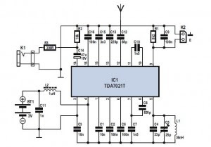
FM Radio Receiver IC TDA 7012T is very simple, but it has an FM radio receiver sensitivity and good selectivity. Single Chip FM Receifer cool name of IC TDA7012T 7012T TDA is to build an FM receiver requires a few additional components. 
Feature contained in FM receiver IC TDA 7012T is quite tempting to an FM receiver. Among features an FM receiver TDA 7012T is a low-voltage applications micro affability arrangement (MTS), Frequency Loked Loop (FLL) to 76 KHz range and selectivity of FM receiver with RC Filter. In an article by FM Radio Receiver IC TDA 7012T can be seen in the FM receiver circuit which can be made​​.


FM Radio Receiver with IC TDA 7012T

From the picture above components to make the FM Radio Receiver IC TDA 7012T as follows:

R1 = 8kΩ2
R2 = 10kΩ
R3 = 390Ω
C1, C3 = 10nF
C2, C6, C9, C16 = 100nF
C4 = 33pF
C5 = 25pF trimmer
C7, C10 = 1nF5
C8 = 820pF C11 = 1NF
C12 = 68pF
C13 = 220pF
C14 = 47μF 10V
C15 = 3nF3
L1 = 36nH
L2 = 1μH,
IC1 = TDA7021T

Hopefully useful and become an idea in the manufacture of Mini FM Receiver with IC TDA 7012T
Read More..

Tuesday, November 18, 2014

Police Sirine Circuit with IC 555

The series of police sirens with 555 ic this is a series of sirens that utilizes two IC 555 as a pulse generator and producing shrill voice. 

Police
Both ic 555 respectively build the astable multivibrator circuit and generate output signals with different frequencies. It is intended to be used as one of the high frequency generator or a screeching sound and the other as a regulator of the swing from last shrill voice. If we observe the working principle of this circuit is very similar to a series of modulation fm. Where the shrill sound signal likened to a high frequency signal from the oscillator circuit and control signal swing is the wail of the information signal or input signals that will transmit. This is consistent with the shape of the output signal associated with the loudspeaker, which has an output signal frequency changes in the form of regular meetings wave tenuous.

Actually a series of sirens could be simpler than if you use a 556 IC which is a dual multivibrator or equal to two pieces of IC 555. IC 556 has two multivibrator circuit menfaatkan so you can meet the workflow of this siren sound-producing circuit. Or you can also make it by using a combination of multiple transistors. And it could be you do remember the oscillator circuit can be easily made with transistors.

Appropriate image above then:
R1, R2, and C1 is a determinant of the frequency of the signal generated by IC1
R3, R4 and C3 is a determinant of the signal frequency whine
Signals generated by IC1 IC2 pin 5 connected to the control signals intended for the resulting shrieks
Screeching sound signal will swing to follow the control of the output signal IC1
You can do experiments in order to gain more understanding of police sirens this circuit by changing the value of some critical components such as the frequency of R1, R2, R3, R4, C1 and C3.
Read More..

Michas AVR Transistor tester

Everyone knows the problem: you have a transistor, but you can not read the signature. Or you can not find the datasheet. You have a diode or you have a capacitor, but you can not read ... Here is the solution smarty.


Michas_AVR-Transistortester

Features:
* Automatic detection of NPN and PNP transistors, N-and P-channel MOSFET, the diode (including the double diode), thyristor, triac and resistor.
* Automatic pin detection and reporting of test components
* Detect and display protection diode and the MOSFET transistor
* Determination of the amplification factor and the forward base-emitter voltage of transistor
* Measurement of threshold voltage and gate capacitance of MOSFET
* Show the value of the text-LCD (2 × 16)
* One-button operation, automatic shut-off
* Power consumption in off mode: <20 na

This tester also supports measuring the diode, R / C testing, and many other components identified.
Read More..

Speaker Protector Circuit with DC Protection

Speaker protector function to protect the speakers from damage caused by spikes in the audio signal when first turned on and the DC signal from the audio signal clipping. circuit protectors speakers consist of 2 parts which can protect the speakers are part of the DC signal detection and the delay. Part detetor DC signal composed by 4 pieces arranged diode bridge and a transistor. Then agian delay on the speaker is using a tank circuit protector in the form of capacitors, where the circuit composed of R6, C3, TR2 and TR3. End part of the speaker is using a relay protector. circuit protectors speakers in detail can be seen in the following figure.

Safety Speaker circuit
speaker

speaker
Component Speaker Protector Protection
Speaker circuit surge protector is equipped with a flashing indicator made ​​for the postponement of the power amplifier to the speakers. Speaker circuit surge protector can be used to protect the speakers in stereo audio system.
Read More..

Function of IC LM35 and How It Works

Do you looking for the function of IC LM35 ? The works of IC LM 35 typically serves as a temperature sensor. IC LM 35 is packaged in the form of integrate circuit which prisoners rates is a function of temperature, the temperature will cause a change of IC LM 35.

Heat energy from the electrodes will cause the IC LM 35 temperature changes that subsequently alter rates prisoners, the characteristics of this sensor is linear to temperature changes means that, if the temperature changes that tend to increase the temperature of the IC will also rise, as well as if the temperature falls.

Images and physical shape of IC LM35
The voltage output from these sensors is ± 10 mu/0C every 10C temperature rise and the largest range of temperatures - 550C to 1150C.
Read More..

Monday, November 17, 2014

Flip Flop LED

Flip flop circuit is a series of free runing multivibrator given the burden of LEDs on each side of the transition changes its output signal. Flip flop circuit with LEDs is quite simple, that is prepared with 2 units and 2 units of 2N3904 transistor circuit tank circuit composed by the RC circuit. LED indicators signal a change that is placed on each side of the flip flop will be lit in turn by the fire and extinguished the same as the charge and discharge capacitor. Flip flop circuit is quite simple as shown in the picture below.

Flip Flop LED series
Flip


The working principle is the flip flop over when the series voltage source is given then the 10uF capacitor will be charged through R 470 and the LED will then be forwarded to triger the transistor base so that the transistor will turn ON and LEDs. this occurs alternately on each side, so that the LED light will illuminate in turn as well.
Read More..

12V to 20V DC Converter Circuit

100 Watt 12V to +/- 20V DC Converter Circuit
DC To DC Converter circuit used to be an convert  voltage DC to DC with different concepts. DC to DC converter circuit +12 V to + /-20V is working to change the battery voltage from 12V DC to 20V DC voltage symmetrical. DC to DC converter circuit is often applied to the power amplifier udio on car audio systems. DC to DC converter circuit uses a TL494 IC as power plsa for the converter. 
TL494 IC is a PWM controller with an adjustable frequency from 40-60Hz through a potentiometer. Then from the TL494 PWM signal is given to the driver MOSFET inverter TPS2811P to be given to the power inverter with 2 units of MOSFET transistors. Circuit details can be seen in the figure following the DC to DC converter.

DC To DC converter circuit +12 V To + / - 20V 

Click to View Larger

List Components DC To DC Converter +12 V To + / - 20V
  • R1, R2 = 10 
  • R3, R4, R6, R7 = 1k 
  • R5 = 22k 
  • R8 = 4.7k 
  • R9 = 100k 
  • C1, C2 = 10000uF 
  • C3, C6 = 47 u 
  • C4 = 10U 
  • C5, C7, C14 = 100n 
  • C8, C9 = 4700u 
  • C12 = 1N 
  • C13 = 2.2u 
  • U1 = TL494 
  • U2 = TPS2811P 
  • Q1, Q2 = FDB045AN 
  • D1-D4 = 1N5822 
  • D5 = 1N4148 
  • FU1 = 10A 
  • L1 = 10U 
  • L2 = ferrite BEAD 
  • RV1 = 2.2k 
  • RV2 = 24k 
  • T1 = TRAN-3P3S 

DC To DC converter circuit +12 V To + / - 20V is capable of supplying up to 100W and can power supplying currents up to 3A. In making DC To DC Converter +12 V To + / - 20V has to be careful and cautious because there are parts of DC To DC Converter +12 V To + / - 20V in the form of an AC circuit.
Read More..

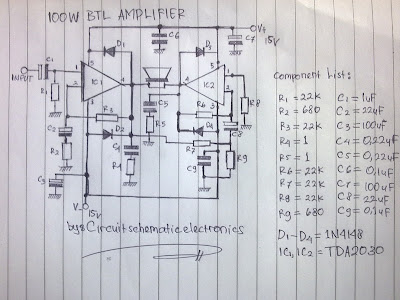
100W BTL TDA2030 amplifier circuit

TDA2030 amplifier circuit using the BTL system has a 100W output power and voltage of +15 V,-15V 0. Amplifier circuit you can see below.

100W
TDA2030 100W amplifier circuit
 .
Read More..

Parts of the UPS Uninterruptible Power Supply


Uninterruptible Power Supply
UPS is basically composed of three main components, namely:
1) Rectifier-Charger
This section is used to transfer circuit and battery charging. Rectifier-charger circuit block is going to supply the power needed by the inverter under full load and at that time to maintain the charge in the battery. Besides these blocks must have the ability to drain the power output of 125-130%.

Characteristics of the batteries also need to be taken into account in its charger circuit design because if a rechargeable battery with a current that exceeds the capacity limit will be able to shorten the life of the battery. Usually for a battery charging current to the UPS is 80% of current conditions issued by the batteries at full load.
Limitation of a UPS system is good by the standards of NEMA - National
Electical Manufacturer Association - is able to provide 100% power continuously (continuous load) and 2 hours at 125% load without a decrease in performance (damage). The battery can still be categorized as unfit for use if the condition is still capable of providing 100% power for 1 hour if the time of filling for 8 hours (determined by the manufacturing
battery).

2) Inverter
The quality of the inverter is a determinant of the quality of power generated by a UPS system. Inverter function to change the DC voltage of the rectifier-charger circuit into AC voltage signal in the form of a sine wave formation and after going through the filter circuit. The resulting output voltage must be stable both voltage amplitude and frequency, low distortion, there are no voltage transients.
In addition, the inverter system needs a feedback circuit (feedback) and the regulator circuit to maintain constant voltage to be obtained.

3) Switch Shifters (Transfer switches)
Transfer switch is divided into two types, namely electromechanical and static. Electromechanical switch uses relays to get one of the supply voltage terminal and the other from the UPS system. Static switch system using semiconductor components, such as SCR.
The use of SCR would be better because of the removal operation is performed with the SCR takes only 3 to 4 ms, while the electromechanical switch is about 50 to 100 ms.
The use of UPS is done by connecting the UPS to the AC input and output PLN UPS to the load. Most UPS are used to supply the computer, because if the source of PLN suddenly dies, then the data being processed is not lost but is still in the back-up by UPS, so theres still time to save data.
Read More..

Sunday, November 16, 2014

BTL Stereo Amplifier TDA7052 3

This is BTL stereo power amplifier with basic amplifier on IC TDA7052 / TDA7053

BTL
Read More..

Saturday, November 15, 2014

OBJECT COUNTER USING 8051

This article is about a simple object counter/visitor counter using 8051 microcontroller . AT89S51 belonging to the 8051 family is the microcontroller used here. This circuit can count the number of objects passing across a line , number of persons passing through a gate/door and so on. The can be simply divided into two sections i.e. the sensor section and the display section.

Sensor

The sensor part consists of a ultra bright led (with focus), and LDR, opamp LM324 and the associated passive components. The LED is placed on one side of the door and the LDR is placed on the other side so that the light from the LED falls directly on the LDR.As you know, the resistance of the LDR has an inverse relationship with the intensity of the light falling on it. The preset resistor R14 is so adjusted that the voltage across the LDR is below 1.5V when it is illuminated. This voltage (labelled A in the circuit diagram) is connected to the inverting input of the opamp which is wired as a comparator with reference voltage 1.5V (set using R15 and R16).Capacitor C1 is meant for bypassing noise or anything like that which may cause false triggering.Resistor R13 is meant to control the current through the LED.
When the light is falling on the LDR the voltage across it will be less than the reference voltage and so the output of the opamp remains high. When the light beam is interrupted, the voltage across the LDR goes above the reference voltage and so the opamp output goes low and it indicates a pass.

Display Section

The output of the opamp is fed to the INTO (interrupt 0) pin of the microcontroller. The microcontroller is programmed to count the number of negative edge pulses received at the INT0 pin and displays it on the three digit seven segment display.

Circuit Diagram


Program

ORG 000H
SJMP INIT
ORG 003H   // starting address of interrupt service routine (ISR)
ACALL ISR   // calls interrupt service routine
RETI

INIT : MOV P0,#00000000B
       MOV P3,#11111111B
       MOV P1,#00000000B
       MOV R6,#00000000B
       MOV DPTR,#LUT
       SETB IP.0 // sets highest priority for the interrupt INT0
      SETB TCON.0 // interrupt generated by a falling edge signal at INT0 pin
       SETB IE.0     //enables the external interrupt
       SETB IE.7     //enables the global interrupt control

MAIN : MOV A,R6
       MOV B,#100D
       DIV AB
       ACALL DISPLAY
       SETB P1.0
       ACALL DELAY
       ACALL DELAY
       MOV A,B
       MOV B,#10D
       DIV AB
       ACALL DISPLAY
       CLR P1.0
       SETB P1.1
       ACALL DELAY
       ACALL DELAY
       MOV A,B
       ACALL DISPLAY
       CLR P1.1
       SETB P1.2
       ACALL DELAY
       ACALL DELAY
       CLR P1.2
       SJMP MAIN

ISR : INC R6   // interrupt service routine
      RET

DISPLAY : MOVC A,@A+DPTR // display sub routine
          CPL A
          MOV P0,A
          RET

DELAY : MOV R3,#255D  // 1mS delay
LABEL : DJNZ R3,LABEL
        RET
LUT : DB 3FH
      DB 06H
      DB 5BH
      DB 4FH
      DB 66H
      DB 6DH
      DB 7DH
      DB 07H
      DB 7FH
      DB 6FH
END

About the Program

The program is written so that, it keeps displaying the current value in register R6 on the three digit seven segment display. When ever there is a valid negative going pulse (interrupt) at the INT0 pin, the program branches to the interrupt service routine (sub routine ISR). Subroutine ISR increments the value in register R6, then jumps back to the MAIN loop and the display gets updated by the new value.

Notes

•Entire circuit can be powered from a 5V DC supply.
•LDR must be placed in an enclosure so that the light from LED alone falls on it.

Read More..

Friday, November 14, 2014

Automatic Water Tap Faucet Valve Controller

Presented here is a simple electronic circuit which can control the valve operation by sensing valid-movements with the help of a Passive Infrared (PIR) motion sensing module. In practice, automatic taps are presence sensors and not motion sensors. They employ “Active Infrared” technology which senses “presence” and not “movement” of objects. However, here an unorthodox “Passive Infrared” technology is used to realize the 6V DC powered smart faucet controller circuit.

Schematic of the Water Valve Controller Circuit


Smart Valve Controller is a combination of four key components

•motion sensor with control electronics
•solenoid valve
•power source
•and the faucet
As stated, at the heart of the circuit is a Passive Infrared (PIR) module. PIR sensor is a pyroelectric device that detects motion by measuring changes in the infrared levels emitted by surrounding objects. Pyroelectric devices, such as the PIR sensor, have elements made of a crystalline material that generates an electric charge when exposed to infrared radiation. The changes in the amount of infrared striking the element change the voltages generated, which are measured by an onboard amplifier.

The device contains a special filter called a Fresnel lens, which focuses the infrared signals onto the element. The PIR Sensor requires a ‘warmup’ time in order to function properly. This is due to the settling time involved in ‘learning’ its environment. this could be anywhere from 10 to 60 seconds. During this time there should be as little motion as possible in the sensors field of view. There is a variable resistor (P1) on the PIR sensor module to control the ‘ON’ delay time for the sensor. Turning this variable resistor clockwise will give longer ‘ON’ delay time while turning anticlockwise will reduce the ‘ON’ delay time. The PIR sensor has distance range of approximately 3 to 7 meters. It is possible to adjust distance of detection with the help of the second variable resistor (P2) on the PIR sensor module.

Likewise, there is a 2-position jumper point (JP) is included in the PIR sensor module. The sensor is active HIGH (LOW in idle state) when jumper is in either position. In “retrigger” (H) position, output remains HIGH when sensor is triggered repeatedly. In “normal” (L) position, output goes HIGH then LOW when triggered. Continuous motion results in repeated HIGH/LOW pulses.

The motion sensor with control electronics circuitry is very simple and self-explanatory. Output of the PIR sensor module (SEN1) is here connected to a ‘traditional’ monostable multivibrator (MMV) wired around the ubiquitous timer chip NE555 (IC1) . Output of IC1 controls the solenoid valve through a 6V electromagnetic relay attached to J1.

Two LEDs (LED 1 & LED2) are added as system status indicators. SPDT switch S1 is the “Auto/Manual” Mode Selector. “Push – to – On” switch S2 can be used for manual operation of the faucet. Prototype tested with four 1.5V AA cells (1.5Vx4 = 6V).

Note


  • Remember to set delay time & detection range of the system as low as possible by adjusting the preset pots P1 & P2 of the PIR sensor module. Removing the fresnel lens, collimation and screening by means of a piece of a suitable electrical conduit with a length of 2 to 3 cm is not a bad idea to reduce the field of view of the PIR sensor module. Place the jumper (JP) in “Normal” mode!
  • Why a PIR sensor based design? PIR sensor is small, inexpensive, low power, rugged,is easy to interface with, and is easy to use. When motion is detected the PIR sensor outputs a high signal on its output pin, which can either be read by an MCU or drive a transistor to switch a higher current load.

Parts List

•SEN 1: PIR sensor module
•T1: BC547
•LED1: 5mm Green
•LED2: 5mm Red
•D1: 1N4007
•IC1: NE555
•R1, R2: 1K
•R3: 100K
•R4: 470R
•C1,C2: 100nF
•C3: 100uF/16V
•S1: SPST On/Off
•S2: Push -To – On
•J1: 2-Pin male header
•Relay: 6VDC /SPST Electromagnetic Relay

Read More..

Thursday, November 13, 2014

Voltage Tester for Model Batteries

With a suitable load, the terminal voltage of a NiCd or lithium-ion battery is proportional to the amount of stored energy. This relationship, which is linear over a wide range, can be used to build a simple battery capacity meter. 

Circuit Image :
 
Voltage Tester for Model Batteries Circuit Image 

This model battery tester has two functions: it provides a load for the battery, and at the same time it measures the terminal voltage. In addition, both functions can be switched on or off via a model remote-control receiver, to avoid draining the battery when it is not necessary to make a measurement. The load network, which consists of a BC517 Darlington transistor (T2) and load resistor R11 (15 Ω /5 W), is readily evident. When the load is active, the base of T1 lies practically at ground level. Consequently, T1 conducts and allows one of the LEDs to be illuminated. 

Circuit Diagram :

Voltage Tester for Model Batteries Circuit Diagram

The thoroughly familiar voltmeter circuit, which is based on the LM3914 LED driver, determines which LED is lit. The values of R6 and R7 depend on the type and number of cells in the battery. The objective here is not to measure the entire voltage range from 0 V, but rather to display the portion of the range between the fully charged voltage and the fully discharged voltage. Since a total of ten LEDs are used, the display is very precise. For a NiCd battery with four cells, the scale runs from 4.8 V to 5.5 V when R6 = R7 = 2 kΩ. The measurement scale for a lithium-ion battery with two cells ranges from 7.2 V to 8.0 V if R6 = 2 kΩ and R7 = 1 kΩ. 

For remote-control operation, both jumpers should be placed in the upper position (between pin 1 and the middle pin). In this configuration, either a positive or negative signal edge will start the measurement process. A positive edge triggers IC1a, whose output goes High and triggers IC1b. A negative edge has no effect on IC1a, but it triggers IC1b directly. In any case, the load will be activated for the duration of the pulse from monostable IC1b. Use P12 to set the pulse width of IC1a to an adequate value, taking care that it is shorter than the pulse width of IC1b. 

If the voltage tester is fitted into a remote-controlled model, you can replace the jumpers with simple wire bridges. However, if you want to use it for other purposes, such as measuring the amount of charge left in a video camera battery, it is recommended to connect double-throw push-button switches in place of JP1 and JP2. The normally closed contact corresponds to the upper jumper position,while the normally open contact corresponds to the lower position.

Parts :
Resistors:
R1,R2 = 47kΩ
R3 = 100kΩ
R4 = 500kΩ
R5 = 1kΩ
R6,R7 = see text (1% resistors!)
R8 = 1kΩ5
R9 = 1kΩ2
R10 = 330Ω
R11 = 15Ω 5W
R12 = 15kΩ
P1 = 100kΩ preset
Capacitors:
C1 = 10nF
C2 = 100nF
Semiconductors:
D1-D10 = LED, red, high effi-ciency
T1 = BC557
T2 = BC517
IC1 = 74HC123
IC2 = LM3914AN
Miscellaneous:
PC1,PC2,PC3 = solder pin
JP1,JP2 = jumper or pushbuttonPCB Layout :

Voltage Tester for Model Batteries PCB Layout
Read More..

50W audio amplifier LM3876

LM3876 is a high performance audio power amplifier IC from National Semiconductors. The LM3876 can deliver 50watts of output power into an 8 ohm loudspeaker. LM3876 has excellent signal to noise ratio and has wide supply voltage range. Other features of LM3876 are output to ground short circuit protection, input mute function, and output over voltage protection, etc. Applications of LM3876 are component stereo, compact stereo, surround systems, self powered speakers, etc.
Circuit diagram :

50W audio amplifier Circuit Diagram
The 50 watt audio amplifier  circuit shown below is designed based on the application diagram from the data sheet of LM3876. Some modifications are made on the original circuit for improving the performance. The bipolar electrolytic capacitor C7 is the input DC decoupling capacitor. R4 is the input resistance. R2 & R1 and bipolar electrolytic capacitor C5 forms a feedback circuit. C2, C1 are filter/by-pass capacitors for the positive supply rail. C4 & C3 are the filters/by-pass capacitors for the negative supply rail. The feedback resistor R2 sets the gain of the amplifier. L1 provides high impedance at high frequencies so that R7 may decouple capacitive loads. R3 is the mute resistance which allows 0.5mA to be drawn from pin8 to turn the mute function OFF. S1 is the mute switch. Resistor R6 and capacitor C8 forms a Zobel network which improves the high frequency stability of the amplifier and prevents oscillations.
Notes :
  • The LM3876 can be operated from a supply voltage range of +/-12V to +/-49V DC.
  • I recommend +/-35V DC for powering the IC.
  • LM3876 requires a proper heat sink.
  • Quiescent current of LM3876 is around 70mA
Read More..

Burglar Alarm Using LDR and BC 548

Description               Circuit showing a Burglar Alarm.Here we have used a ldr and a switching transistor for making this circuit
.When the light coming towards the ldr during the period the ldr have low resistance so the buzzer will on.When the light going away the ldr during the period the ldr have high resistance so the transistor will off.Here you need a 12 volt power supply

 Components Required      Resistor

                   10 k(preset)

      Transistor
                   BC 548

       LDR
        Buzzer

Source by : http://www.electronics-circuits.in/2012/03/burglar-alarm-ldr-bc-548.html
Read More..

Ceiling Fan Regulator Circuit Motor Speed Controller

This is a simple ceiling fan regulator circuit diagram tutorial. It is used to control the speed of a ceiling fan. In the other words it is an AC motor speed controller circuit, as because its control the speed of a AC motor(Ceiling Fan).  This ceiling fan regulator circuit built with few numbers of parts. The circuit mainly  based on Z0607 TRIAC. This is a low power AC semiconductor device. Generally which is used to controlling speed of low power ac motor speed. 

Circuit Diagram of Ceiling Fan Regulator :


Ceiling
Fig: Ceiling fan regulator (AC motor speed controller)  Circuit Diagram

In this ceiling fan regulator circuit, R1=500KΩ is a variable resistor that is used to adjust the fan speed. Capacitor C1 2A104J is a Polyester film capacitor.

Pin Diagram of  TRIAC(T1)- Z0607: 


Z0607
Fig: Z0607-TRIAC Pin diagram

Pin Diagram of Variable Resistor R1:


Fig: Pin Diagram of Variable Resistor

Parts List Of Ceiling Fan-Motor Speed Controller circuit:

T1 = Z0607 -TRIAC
D1 = DB3 C312 -DIAC
R1 = 500KΩ -Variable Resistor
R2 = 37KΩ -Resistor
C1 = 2A104J -Polyester film capacitor.
M1 = Single Phase AC Motor (Ceiling Fan)-220V,50Hz
Read More..

Wednesday, November 12, 2014

Remote Operated Home Appliances Circuit

Here is the circuit diagram of Remote Operated Home Appliances or Remote controlled Home appliances. Connect this circuit to any of your home appliances (lamp, fan, radio, etc) to make the appliance turn on/off from a TV, VCD, VCR, Air Conditioner or DVD remote control. The circuit can be activated from up to 10 meters. It is very easy to build and can be assembled on a veroboard or a general-purpose PCB.

Circuit diagram:

Remote Control For Home Appliances

Parts:

R1 = 220K
R2 = 330R
R3 = 1K
R4 = 330R
R5 = 47R
C1 = 100uF-16V
C2 = 100nF-63V
C3 = 470uF-16V
D1 = 1N4007
D2 = Red LED
D3 = Green LED
Q1 = BC558
Q2 = BC548
IR = TSOP1738
IC1 = CD4017
RL1 = Relay 5V DC

Circuit Operation:
The 38kHz infrared rays generated by the remote control are received by IR receiver module TSOP1738 of the circuit. Pin 1 of TSOP1738 is connected to ground, pin 2 is connected to the power supply through R5 and the output is taken from pin 3. The output signal is amplified by Q1. The amplified signal is fed to clock pin 14 of decade counter IC CD4017 (IC1). Pin 8 of IC1 is grounded, pin 16 is connected to vcc and pin 3 is connected to D2 (Red LED), which glows to indicate that the appliance is ‘off.’

The output of IC1 is taken from its pin 2. D3 connected to pin 2 is used to indicate the ‘on’ state of the appliance. Q2 connected to pin 2 of IC1 drives relay RL1.
D1 acts as a freewheeling diode. The appliance to be controlled is connected between the pole of the relay and neutral terminal of mains. It gets connected to live terminal of AC mains via normally opened (N/O) contact when the relay energizes. If you want to operate a DC 12 volt relay then use a regulated DC 12 volt power supply for DC 12 volt Relay and remember that the circuit voltage not be exceeded more than DC 5 volte.
Read More..

using 555 timer ic White led driver circuit with explanation

 using 555 timer ic white led driver circuit with explanation
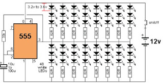
A very simple white led driver electronic circuit project can be designed using this circuit diagram , that is based on a 555 timer circuit and some other electronic parts .
The 555 is capable of sinking and sourcing up to 200mA, but it gets very hot when doing this on a 12v supply.

This white led driver circuit shows the maximum number of white LEDs that can be realistically driven from a 555 timer . The total current was limited to about 130mA as each LED is designed to pass about 17mA to 22mA maximum. A white LED drops a characteristic 3.2v to 3.6v and this means only 3 LEDs can be placed in series.
As you can see in the circuit diagram , this electronic project circuit require few external electronic parts and is capable to drive up to 48 white LEDs from a 12 volts DC power source , utilizing few electronic components .
Read More..

IC TDA7012T Mini FM Received Based on Single FM circuit with explanation

 ic tda7012t mini fm received based on single fm circuit with explanation
Mini FM Received Circuit

TDA7021T chip radio receiver ambit is for carriageable radios, stereo as able-bodied as mono, area a minimum of ambit is important in agreement of baby ambit and low cost. It is absolutely accordant for applications application the low-voltage micro affability arrangement (MTS). The IC has a abundance bound bend (FLL) arrangement with an average abundance of 76 kHz. The selectivity is acquired by alive RC filters.

The alone action to be acquainted is the beating abundance of the oscillator. Interstation babble as able-bodied as babble from accepting anemic signals is bargain by a alternation aphasiac system.

Part List:

R1 = 8kΩ2
R2 = 10kΩ
R3 = 390Ω
C1,C3 = 10nF
C2,C6,C9,C16 = 100nF
C4 = 33pF
C5 = 25pF trimmer (Murata type TZB4Z250AB10R00)
C7,C10 = 1nF5
C8 = 820pF C11 = 1nF
C12 = 68pF
C13 = 220pF
C14 = 47μF 10V (Nichicon UWX1A470MCL1GB 5.5mmL chip type)
C15 = 3nF3
L1 = 36nH (4 turns 0.5mm silver-plated wire, inside diameter 4mm; length 7mm)
L2 = 1μH, SMD case 0805 (fres > 300 MHz)
IC1 = TDA7021T (SMD in SO16 case)

Read More..

Simple Police Siren

The simple Police Siren circuit uses two 555s to produce an up-down wailing sound. The first 555 is wired as a low-frequency oscillator to control the VOLTAGE CONTROL pin 5 of the second 555. The voltage shift on pin 5 causes the frequency of the second oscillator to rise and fall.Simple Police Siren Circuit Diagram
Read More..

Tuesday, November 11, 2014

How to Build a Shake Tic Tac LED Torch

In the diagram, it looks like the coils sit on the “table” while the magnet has its edge on the table. This is just a diagram to show how the parts are connected. The coils actually sit flat against the slide (against the side of the magnet) as shown in the diagram:


 Shake Tic Tac LED Torch Circuit Diagram

The output voltage depends on how quickly the magnet passes from one end of the slide to the other. Thats why a rapid shaking produces a higher voltage. You must get the end of the magnet to fully pass though the coil so the voltage will be a maximum. That’s why the slide extends past the coils at the top and bottom of the diagram.

The circuit consists of two 600-turn coils in series, driving a voltage doubler. Each coil produces a positive and negative pulse, each time the magnet passes from one end of the slide to the other.
The positive pulse charges the top electrolytic via the top diode and the negative pulse charges the lower
electrolytic, via the lower diode.

The voltage across each electrolytic is combined to produce a voltage for the white LED. When the combined voltage is greater than 3.2v, the LED illuminates. The electrostatics help to keep the LED illuminated while the magnet starts to make another pass.
Read More..

Courtesy Light Extender

In essence, this circuit is a 15 to 20-second courtesy light extender for cars. It is activated in the usual way by opening a door but it also samples the negative lock/unlock signals from a car alarm or central locking and does two more things. First, when an unlock signal is received, it turns on the courtesy light for 15-20 seconds before you open the door. Second, when a lock signal is received, it turns off the courtesy light immediately, with no fade-out. This is done to eliminate false triggering of the burglar alarm through current drain sensing. When a car door is open or the unlock relay is activated, the 33µF capacitor discharges through diode D1 and this keeps transistor Q1 turned off.

Circuit diagram:


 Courtesy Light Extender Circuit Diagram

This allows Q2 and Q3 to turn on and the courtesy lamp is activated. When the door is closed, the courtesy lamps stay illuminated and the 33µF electrolytic capacitor starts charging through the associated 1MO resistor. As the voltages rises, Q1 turns on slowly, turning off Q2 and Q3 which gradually fades out the courtesy lamp. If a lock signal from the central locking system is received, relay 1 closes and charges the capacitor instantly, so the lamp turns off immediately. Relays were used to interface to the central locking/alarm system as a safety feature, to provide isolation in case something goes wrong.
Author: Matt Downey - Copyright: Silicon Chip Electronics
Read More..

Sunday, November 9, 2014

A Car Battery Monitor

A close call on the road can really focus your mind on the importance of having a battery monitor in a car. I had been enjoying a pleasant week of travelling around the countryside at a leisurely pace and taking in the beautiful scenery each day. It wasnt until the final day, with the big rush to return home, that I had to drive at night.My home is deep in the country and on the road I was travelling the closest petrol station may be 80km away. I was travelling through an area that is full of open-cut coal mines and large heavily loaded semi-trailers constantly pound the roads, travelling at quite high speeds. It was around 8pm at night and everything was very dark no street lights or house lights anywhere.

Just as I was going up a hill, the lights began to dim and the engine coughed. A large semi-trailer loomed in the rear-vision mirror as I pushed the clutch in and tried to restart. My speed was falling rapidly and my lights were blacked out - I was like a sitting duck in the middle of the road, as the semi-trailer came rapidly bearing down on me. I just managed to pull the car off the road, as the semi-trailer came screaming past, missing me by inches! After calling for assistance from the NRMA, the problem was found to be a fault in the alternator, which was failing to charge the battery. The battery voltage had been falling under the heavy load of the lights and at the worst possible time, there was not sufficient power for the lights or the motor.

After the initial shock wore off, I put on my thinking cap to come up with a PIC-based solution to the problem. What was really needed was a display and a buzzer, to get my attention should the voltage fall outside a specified range. So my design criteria was set, a series of LEDs could indicate the voltage and a buzzer would also be used to warn of problems.
Main Features:
  • Visual indication of battery voltage
  • Audible warning when voltage becomes low
  • Screw terminals for easy connection
  • Simple and easy to build
Circuit details:

The circuit is based on PIC16F819 18-pin microcontroller which has an analog-to-digital (A/D) input to monitor the battery voltage and outputs capable of driving LEDs directly, to keep the component count down. There are seven LEDs in all, giving a good range of voltage indication. The topmost LED, LED1, comes on for voltages above 14V which will occur when the battery is fully charged. LED2 indicates for voltages between 13.5V and 14V while LED3 indicates between 13V and 13.5V. Normally, one of these LEDs will be on. LED4 covers 12.5V to 13V while LED5 covers 12V to 12.5V. LED6 covers from 11.5V to 12V while LED7 comes on for voltages below 11.5V. These two LEDs are backed up by the piezo chime which beeps for voltages between 11.5V and 12V and becomes more insistent for voltages below 11.5V.

That might seem fairly conservative. After all, most cars will start with no troubles, even though the battery voltage might be a touch below 12V, wont they? Well, no. Some modern cars will happily crank the motor at voltages below 11V but their engine management will not let the motor start unless the voltage is above 11V. So dont think that a modern car will always start reliably. This little battery monitor could easily prevent a very inconvenient failure to start! So lets describe the rest of the circuit. The incoming supply is connected via diode D1 which provides protection against reverse polarity while zener diode ZD1 provides protection from spike voltages.

A standard 7805 3-terminal regulator is then used to provide a stable 5V to the microcontroller. The battery voltage is sensed via a voltage divider using 33kΩ and 100kΩ resistors. This brings the voltage down to within the 0-5V range for the A/D input of the PIC16F819. Port B (RB0 to RB7) of the microcontroller is then used to drive the various LEDs, with current limiting provided via the 330Ω resistor network. RB7, pin 13, drives a switching transistor for the piezo buzzer.

Software:
For the software, the design follows the basic template for a PIC microcontroller. Port A and its ADC (analog-to-digital converter) function are set up while port B functions as the output for the LEDs and buzzer. Once the set-up is complete, a reading will be taken at port RA2, the input for the A/D convertor. This reading is then compared with a series of values to determine the range of the voltage. This is similar to a series of "if" statements in Basic language. If the voltage is found to be within a certain range, the relevant port B pin will be turned on. If the voltage is below 12V, the buzzer will be turned on for a brief period, to signal a low battery condition. As the voltage falls below 11.5V, the frequency of the beeps will increase, to signal increased urgency.

Building it:

All the parts are mounted on a small PC board measuring 46 x 46mm (available from Futurlec). The starting point should be the IC socket for the PIC16F819, as this is easiest to mount while the board is bare. The next item can be the PC terminal block. The resistors and capacitors can then follow. Make sure the electrolytics are inserted with correct polarity.

Make sure that you do not confuse the zener (ZD1) with the diode when you are installing them; the diode is the larger package of the two.
Even more important, dont get the 78L05 3-terminal regulator and the 2N3906 transistor mixed up; they come in identical packages. The 78L05 will be labelled as such while the 2N3906 will be labelled "3906". And make sure you insert them the correct way around. The buzzer must also be installed with the correct polarity. The 330Ω current limiting resistors are all in a 10-pin in-line package. There are four green LEDs, two yellow and one red. They need to be installed in line and with the correct orientation.

Testing:

Before you insert the PIC16F819 microcontroller, do a voltage check. Connect a 12V source and check for the presence of 5V between pins 14 & 5 OF IC1. If 5V is not present, check the polarity of regulator REG1 and the polarity of the diode D1. If these tests are OK, insert the IC and test the unit over a range of voltage between 9V and 15V. Make sure that all LEDs come on in sequence and the piezo buzzer beeps for voltages below 12V. 

Now it is matter of installing the unit in your car. It is preferable to install the unit in a visible position for the driver. However, it should not obscure any other instruments. The unit should be connected to the cars 12V supply after the ignition switch. This will turn the unit off with the other instruments and prevent battery drain while the motor is not running.

Read More..

Saturday, November 8, 2014

Telephone Number Display Circuit Diagram


The given circuit, when connected in parallel to a telephone, dis- plays the number dialled from the telephone set using the DTMF mode. This circuit can also show the number dialled from the phone of the called party. This is particularly helpful for receiving any number over the phone lines. The DTMF signal—generated by the phone on dialling a number—is decoded by DTMF decoder CM8870P1 (IC1), which converts the received DTMF signal into its equivalent BCD number that corresponds to the dialled number. This binary number is stored sequentially in 10 latches each time a number is dialled from the phone. The first number is stored in IC5A (1/2 of CD4508) while the second number is stored in IC5B and so on.

The binary output from IC1 for digit ‘0’ as decoded by IC1 is 10102 (=1010), and this cannot be displayed by the seven-segment decoder, IC10. Therefore the binary output of IC1 is passed through a logic-circuit which converts an input of ‘10102’ into ‘00002’ without affecting the inputs ‘1’ through ‘9’. This is accomplished by gates N13 through N15 (IC11) and N1 (IC12). The storing of numbers in respective latches is done by IC2 (4017). The data valid output from pin 15 of IC1 is used to clock IC2. The ten outputs of IC2 are sequentially connected to the store and clear inputs of all the latches, except the last one, where the clear input is tied to ground. When an output pin of IC2 is high, the corresponding latch is cleared of previous data and kept ready for storing new data. Then, on clocking IC2, the same pin becomes low and the data present at the inputs of that latch at that instant gets stored and the next latch is cleared and kept ready.

The similar input and output pins of all latches are connected together to form two separate input and output buses. There is only one 7-segment decoder/driver IC10 for all the ten displays. This not only reduces size and cost but reduces power requirement too. The output from a latch is available only when its disable pins (3 and 15) are brought low. This is done by IC3, IC12 and IC13. IC3 is clocked by an astable multivibrator IC4 (555). IC3 also drives the displays by switching corresponding transistors. When a latch is enabled, its corresponding display is turned on and the content of that latch, after decoding by IC10, gets displayed in the corresponding display. For instance, contents of IC5A are displayed on display ‘DIS1,’ that of IC5B on ‘DIS2’ and so on. The system should be connected to the telephone lines via a DPDT switch (not shown) for manual switching, otherwise any circuit capable of sensing handset’s off-hook condition and thereby switching relays, etc. can be used for automatic switching.

The power-supply switch can also be replaced then. Though this circuit is capable of showing a maximum of ten digits, one can reduce the display digits as required. For doing this, connect the reset pin of IC2, say, for a 7-digit display, with S6 output at pin 5. The present circuit can be built on a veroboard and housed in a suitable box. The displays are common-cathode type. To make the system compact, small, 7-segment displays can be used but with some extra cost. Also, different colour displays can be used for the first three or four digits to separate the exchange code/STD code, etc.  
Read More..

Dual High Side Switch Controller

Circuit diagram :

Dual High Side Switch Controller Circuit Diagram


One of the most frequent uses of n-channel MOSFET’s is as a voltage controlled switch. To ensure that the MOSFET delivers the full supply voltage to the load it is necessary for the gate voltage to be a few volts above the supply voltage level. This can be a problem if no other suitable higher volt-age sources are available for use elsewhere in the circuit. The LTC 1982 dual high-side switch controller from Lin-ear Technology (www.linear-tech.com) solves this problem by incorporating a voltage tripler circuit in the gate driver stage. The gate voltage is limited to +7.5 V which is 2.0 V above the IC’s maximum operating voltage. It can directly drive the gate of logic-level MOSFET with a VGS(th) from 1.0 V to 2.0 V. A suitable n-channel logic level MOSFET would be the BSP 295. This device can switch up to 1.5 A and is available in an SOT 233 SMD package.
Read More..

Solar Panel Current Meter

This circuit is used to measure the current from a solar panel. It has very low power loss for currents in the 0-10A range. It also works as a general purpose DC current meter. The circuit can be used on either the positive or negative side of a DC circuit.

Solar Panel Current Meter


Specifications


Measured Current: 0-10 Amps DC
Circuit Voltage: Will work with DC circuits at any practical voltage.
Accuracy: approximately 2%, depending on the meter movement.

Theory


The current to be measured flows through the 0.01 ohm resistor which causes a small voltage drop across the resistor. The 100 microamp meter is set up with the series 50 ohm and 500 ohm variable resistor in a voltage measurement configuration to measure this voltage drop. The 500 ohm variable resistor is used to adjust the meters full scale reading. The 50 ohm resistor limits the maximum current to the meter no matter what setting is on the 500 ohm resistor, this protects the meter from passing too much current and burning up. The series resistance of the meter, 500 ohm (or less) variable resistor and 50 ohm resistor should total 1000 ohms. Different meters may require a different variable resistor to achieve the 1000 ohm value.

Construction


Build the meter into a metal box with the meter and two connectors mounted on the outside of the box.

Alignment


Put the meter circuit in series with a known current meter such as a digital VOM meter set to measure current. Run a known current through both meters. Adjust the 500 ohm resistor until both meters read the same current. A good way to get a known current is to put a 12V lead acid battery in series with a 2 ohm 100 watt current limiting resistor. This will produce approximately 6 Amps of current. Put the two meters in series with this loop and adjust for the same reading. Beware, the resistor will get fairly hot in a short time.

Use


Connect this circuit in series with a nominal 12V or 24V solar panel array. The meter can go in either the positive or negative side of the solar panel circuit. The current flowing through the solar panel to the load will be shown on the meter.

Parts


1x 100 microamp DC meter
1x 0.01 ohm 5 W resistor
1x 50 ohm 1/4 W resistor
1x 500 ohm 10 turn variable resistor
2x banana plugs or a 2 pin screw type terminal block.
1x metal box
Read More..

Acoustic Distress Beacon

An ELT (Emergency Locator Transmitter, also known as a distress beacon) is an emergency radio transmitter that is activated either manually or automatically by a crash sensor to aid the detection and location of aircraft in distress. This acoustic ELT project is intended for radio control (RC) model aircraft, which every now and then decide to go their own way and disappear into the undergrowth.
Circuit diagram :
Acoustic Distress Beacon Circuit Diagram

The audio locating device described here enables model aircraft that have landed ‘off limits’ to be found again and employs its own independent power supply. The small cam-era battery shown in the circuit activates an acoustic sounder when radio contact is lost and produces a short signal tone (bleep) every ten seconds for more than 25 hours. Current consumption in standby and passive (with jumper J1 set) modes is negligible. The timing generator for the alarm tone is the Schmitt trigger AND-gate IC1.B; its asymmetric duty cycle drives a 5 V DC sounder via MOSFET transistor T1. All the time that the RC receiver output is delivering positive pulses, the oscillator is blocked by IC1.A and diode D1. Setting jumper J1 parallel to C2 also disables the oscillator and serves to ‘disarm’ the distress beacon.
Read More..

Friday, November 7, 2014

Motorbike Alarm

This simple to build alarm can be fitted in bikes to protect them from being stolen. The tiny circuit can be hidden anywhere, without any complicated wiring. Virtually, it suits all bikes as long as they have a battery. It doesnt drain out the battery though as the standby current is zero. The hidden switch S1 can be a small push-to-on switch, or a reed switch with magnet, or any other similar simple arrangement. The circuit is designed around a couple of low-voltage MOSFETs configured as monostable timers. Motorbike key S2 is an ignition switch, while switch S3 is a tilt switch. Motorbike key S2 provides power supply to the gate of MOSFET T2, when turned on. 
When you turn ignition off using key S2, you have approximately 15 seconds to get off the bike; this function is performed by resistor R6 to discharge capacitor C3.

Thereafter, if anyone attempts to get on the bike or move it, the alarm sounds for approximately15 seconds and also disconnects the ignition circuit. During parking, hidden switch S1 is normally open and does not allow triggering of mosfet T1. But when someone starts the motorbike through ignition switch S2, MOSFET T2 triggers through diode D1 and resistor R5. Relay RL1 (12V, 2C/O) energises to activate the alarm (built around IC1) as well as to disconnect the ignition coil from the circuit. Disconnection of the ignition coil prevents generation of spark from the spark plug. Usually, there is a wire running from the alternator to the ignition coil, which has to be routed through one of the N/C1 contacts of relay RL1 as shown in Fig.1 Fig.2 shows the pin configurations of SCR BT169, MOSFET BS170 and transistor BC548.
Circuit diagram :

 Motorbike Alarm Circuit Diagram
Motorbike Alarm-Pin Configurations :

Pin configurations of BT169, BS170 and BC548
 
Also, on disconnection of the coil, sound generator IC UM3561 (IC1) gets power supply through N/O2 contact of relay RL1. This drives the darlington pair built around T3 and T4 to produce the siren sound through loudspeaker LS1.  To start the vehicle, both hidden switch S1 and ignition key S2 should be switched on. Otherwise, the alarm will start sounding. Switching on S1 triggers SCR1, which, in turn, triggers MOSFET T1. MOSFET T1 is configured to disable MOSFET T2 from functioning. As a result, MOSFET T2 does not trigger and relay RL1 remains de-energised, alarm deactivated and ignition coil connected to the circuit.  Connection to the ignition coil helps in generation of spark from the spark plug. Keeping hidden switch S1 accessible only to the owner prevents the bike from pillaging.

Tilt switch S3 prevents attempt to move the vehicle without starting it. Glass-and metal-bodied versions of the switch offer bounce-free switching and quick break action even when tilted slowly. 
Unless otherwise stated, the angle by which the switch must be tilted to ensure the contact operation (operating angle), must be approximately 1.5 to 2 times the stated differential angle. The differential angle is the measure of the just closed position to the just open position. The tilt switch has characteristics like contacts make and break with vibration, return to the open state at rest, non-position sensitivity, inert gas and hermetic sealing for protection of contacts and tin-plated steel housing. If you find difficulty in getting the tilt switch, you may replace it with a reed switch (N/O) and a piece of magnet. The magnet and the reed switch should be mounted such that the contacts of the switch close when the bike stand is lifted up from rest.
Read More..