Showing posts with label build. Show all posts
Showing posts with label build. Show all posts
Tuesday, November 11, 2014
How to Build a Shake Tic Tac LED Torch
In the diagram, it looks like the coils sit on the “table” while the magnet has its edge on the table. This is just a diagram to show how the parts are connected. The coils actually sit flat against the slide (against the side of the magnet) as shown in the diagram:

The output voltage depends on how quickly the magnet passes from one end of the slide to the other. Thats why a rapid shaking produces a higher voltage. You must get the end of the magnet to fully pass though the coil so the voltage will be a maximum. That’s why the slide extends past the coils at the top and bottom of the diagram.
The circuit consists of two 600-turn coils in series, driving a voltage doubler. Each coil produces a positive and negative pulse, each time the magnet passes from one end of the slide to the other.
The positive pulse charges the top electrolytic via the top diode and the negative pulse charges the lower
electrolytic, via the lower diode.
The voltage across each electrolytic is combined to produce a voltage for the white LED. When the combined voltage is greater than 3.2v, the LED illuminates. The electrostatics help to keep the LED illuminated while the magnet starts to make another pass.
Read More..
Shake Tic Tac LED Torch Circuit Diagram
The output voltage depends on how quickly the magnet passes from one end of the slide to the other. Thats why a rapid shaking produces a higher voltage. You must get the end of the magnet to fully pass though the coil so the voltage will be a maximum. That’s why the slide extends past the coils at the top and bottom of the diagram.
The circuit consists of two 600-turn coils in series, driving a voltage doubler. Each coil produces a positive and negative pulse, each time the magnet passes from one end of the slide to the other.
The positive pulse charges the top electrolytic via the top diode and the negative pulse charges the lower
electrolytic, via the lower diode.
The voltage across each electrolytic is combined to produce a voltage for the white LED. When the combined voltage is greater than 3.2v, the LED illuminates. The electrostatics help to keep the LED illuminated while the magnet starts to make another pass.

Tuesday, November 4, 2014
Simple Build Telephone Ring Repeater
Even though cordless phones have invaded our homes and offices, you don’t always have them at hand, and as their ringtones are usually very much quieter than the old rotary-dial- type analogue phones, it can happen that you miss a call you’ve been waiting for while you’ve been going about your daily business.
Until quite recently, you could still find remote ringers that could be plugged into any standard phone socket in order to have an additional ringer, but it seems as if these accessories are currently being phased out as everyone is ‘going cordless’. So we decided to suggest something better, with this phone ring repeater that makes it possible to control any device connected to the AC power outlet using the ringtone available on any subscriber line, and naturally, with all the guarantees of safety and isolation that are of course rightly expected. So it’s capable of driving a ringer, or indeed even a high-powered sounder to alert you when you are in the garden, for example; but it is equally able to light a lamp for a ‘silent ring’ so as to avoid waking a sleeping baby or elderly person.
This circuit has been designed to be compatible with all phone systems the author is aware of and also to be totally stand-alone. What’s more, the circuit can be connected to the phone system without any danger though in some countries, it is forbidden to connect non-approved devices to the public switched telephone network (PSTN). Check local regulations in this respect. In order to understand the principle of it, we just need to remember that the ringtone present on a phone installation is an alternating voltage, whose amplitude and frequency vary somewhat between countries, but always with comparable orders of magnitude except in the case of exchange systems used in large companies.
However, when the line is quiescent or a call is in progress, it carries only a direct voltage. Capacitor C1 makes it possible to pick off just the AC ringing volt-age, which is then rectified by D2 and amplitude-limited by D1. The resulting DC voltage charges capacitor C2, which makes it possible to light LED D3 as well as the LED in the optocoupler IC1. This is no ordinary optocoupler, but is in fact an AC power zero-crossing detecting optotriac, which allows us to con-trol the chosen load while generating no, or less, interference, which would not be the case using a standard optotriac.
The output triac it contains is not powerful enough to drive a load directly connected to the mains, so it is used to drive the trigger of triac TRI1, which is a totally standard 400 V device, rated at x amps, where x is chosen to suit the maximum power of the load you want to control using this circuit. Resistors and capacitors R5 and C3 on the one hand, and R6 and C4 on the other help, serve to suppress the switching transients, which are already inherently low because of the AC zero-crossing switching provided by IC1.
Construction is not at all difficult, but does require a few precautions in choosing some of the components. First of all, capacitor C1 must be an MKT type, mylar or equivalent, with a 250 V operating voltage because of the relatively high amplitude of the ringing voltage. For safety reasons, it is essential that capacitors C3 and C4 are self-healing types intended for AC power use at 250 VAC. These capacitors are generally known as Class X or X2 capacitors.
As for the triac, it should have a 400 V operating voltage (but see below for users on 120 VAC power) and maximum current slightly greater than the maximum current drawn by the load being driven. As this will usually be a sounder or a common lamp, a 2 A type will usually be more than adequate in most situations. As the circuit can be expected to operate for short periods only, there is no need to mount the triac on a heatsink. One final important point: as the right hand part of the circuit is connected directly to AC power, it is vital to fit this inside a fully-insulated housing, for obvious safety reasons. Make sure you cannot touch any part when the circuit is in use.
The circuit should work at once and without any problems, but if you notice that D3 doesn’t light up fully, and hence incorrect or erratic triggering of the triac, because of too low a ringing voltage, all you need to put things to rights is reduce the value of resistor R1. The circuit as shown was dimensioned for operation from 230 VAC power. Readers on 120 VAC power should modify the following component values: R4 = 180 Ω; R5 = 220 Ω; TRI = 200 V model; IC1 = MOC3031. Option-ally, C3 and C4 may be rated at 120 VAC.
Friday, October 17, 2014
Build a PIC Security System Dials Your Cell Phone Circuit Diagram
This is a simple PIC Security System Dials Your Cell Phone Circuit Diagram. Do-it-yourself phone dialer security system calls your cell phone, office etc. whenever a door or window is opened, or panic button is pressed. Great Home Alarm.
PIC Security System Dials Your Cell Phone Circuit Diagram
![PIC]()
The circuit consists of a small PIC microcontroller, assembly program, and a few other parts to detect a switch closure from an open door, window, or manual push button and then dial the cell phone number, and transmit a steady tone to indicate the source of the call. The circuit uses the pulse dialing system to interrupt the line connection a number of times to indicate each digit. Pulse dialing (the oldest form of dialing) works by actually disconnecting or "hanging up" the phone line a number of times to indicate each digit. For example, the digit "5" would be dialed by disconnecting and reconnecting the line 5 times in short intervals of about 100mS. There is about a 1 second pause (with the line connected) between each digit. The timing is not critical and I was able to dial 411 and connect to the local information service just using a momentary push button switch in series with the phone line.
PIC Security System Dials Your Cell Phone Circuit Diagram

The circuit consists of a small PIC microcontroller, assembly program, and a few other parts to detect a switch closure from an open door, window, or manual push button and then dial the cell phone number, and transmit a steady tone to indicate the source of the call. The circuit uses the pulse dialing system to interrupt the line connection a number of times to indicate each digit. Pulse dialing (the oldest form of dialing) works by actually disconnecting or "hanging up" the phone line a number of times to indicate each digit. For example, the digit "5" would be dialed by disconnecting and reconnecting the line 5 times in short intervals of about 100mS. There is about a 1 second pause (with the line connected) between each digit. The timing is not critical and I was able to dial 411 and connect to the local information service just using a momentary push button switch in series with the phone line.
Circuit Operation:
In operation, the switch closure is detected on pin 7 of the processor which activates the reed relay and takes the line off-hook for 3 seconds to establish the dial tone. The processor then dials the number by opening and closing the relay a number of times for each digit. When dialing is complete, the processor waits 3 seconds and then transmits a steady tone of about 300Hz for 30 seconds through the modem transformer. The call is then terminated and the processor waits for the switch to open before resetting.
Design Considerations:
The PIC16F628 (18 pin) processor was selected because I had a few on hand and my homemade hardware programmer only accepts 18 pin devices. A smaller 8 pin device could have been used since only three I/O lines are needed, but the difference in cost is only about $1.50. One of the I/O lines (RA5) is used for programming and is always an input, but can used as a functional input so the switch closure could be detected on this line thus eliminating the need for one pullup resistor. But I elected to use 3 consecutive I/O pins (7,8,9) of the 8 bit port B and leave RA5 pulled up with a extra 10K resistor.
The output pins (8,9) that drive the relay and transformer are limited to 25mA of current each, so an extra transistor (2N2222A) was needed to supply additional current to the relay coil. The transformer resistance is around 100 ohms, so an additional 330 ohm resistor was added in series with pin 9 to limit the transformer current to around 10mA. An LED indicator and 330 ohm resistor were used on pin 8 to observe the dialing activity and indicate the line status. Several of the parts (relay, transformer and blocking capacitor) were obtained from an old 56K modem card.
The schematic shows a 47uF / 50 volt non-polarized capacitor used to block DC current to the transformer, however a regular polarized 50uF cap could be used if correct phone line polarity is observed. The modem was probably designed to work with unknown polarities at different locations, so a non-polarized cap was used. Its possible the cap and 470 ohm resistor can be replaced with a single resistor in series with the line to set the "off hook" line current to around 20mA. This may cause partial saturation of the transformer and reduced audio level, but might work well enough.
The power supply voltage is not critical and a 4.5 volt supply from three AA batteries should work. Or a switching type regulated 5 volt wall transformer can be used. The problem is insuring the relay gets enough voltage to operate. The rest of the circuit should run on reduced voltage. I used a 4.2 volt cell phone charger that worked well.
Softwre
Thursday, October 16, 2014
Build a Pulse Charger for reviving tired Lead Acid batteries
If you own a motorcycle, a motor home, a caravan, a lawn mover, a day cruiser or maybe a vintage car you must at some point had to write off a lead acid battery. When a battery is improperly charged or allowed to self-discharge as occurs during non-use, sulphate crystals build up on the batterys plates. The sulphate preventing the battery from being fully charged and therefore it is unable to deliver its full capacity. When trying to charge a battery in this state it only gets hot and looses water, the gravity of the electrolyte is not increasing to its normal “full charge” state.
Pulse Charger for reviving tired Lead Acid batteries Circuit Diagram

The only thing you do is killing the battery completely. If a battery has a resting voltage of at least 1.8 Volts/cell and no cells are shorted, desalination of its plates can be done. This circuit is an add-on and part for a modification of a normal charger and it takes care of the sulphate problem.
The project: get hold of an old charger, big or small it’s your choice depending on the size of batteries you normally handle (bigger is better). There are some tricks to boost the performance if you need it. Start by ripping out everything except the transformer and the rectifier. Some older chargers are equipped with fin rectifiers, which have high voltage drop and must be replaced. Replace with a rugged bridge rectifier that can cope with the amperes. All wiring on secondary should be short and heavy wire. The rectifier should be bolted to the chassis to keep cool. If the charger have a high/low switch it’s a bonus, if not you can in some cases add a few turns of wire on the secondary winding.
The circuit; a 14-stage ripple counter and oscillator IC 4060 produce a pulse, which is the heartbeat of the circuit. The pulse is feed to the 555 timer that deicide the length of the active output. With the switch you can select long or short pulse output. The output of the 555 timer triggers the zero-cross opt isolator triac driver MOC 3041 via a transistor. This gives the charger transformer a soft start via the triac and the snubber circuit. A small power supply is necessary for the circuit and consists of T1 a transformer 15V 0.1A secondary, a bridge rectifier, a regulator and two caps. Because this project include a charger that is (X) the outcome can differ in performance from one case to another. However this do not mean that your project doesn’t work, but the efficiency can vary. Some notes the snubbercap is a high voltage AC type (X) and the resistors on the mains side is at least 0.5W type. Use a triac that can take 400V+ and 10A+, I use BTA 25.600 but this is overkill in most cases. No PCB sorry!
How it works:
Well the short version. The object is to get the cell voltage high enough for the sulphate to dissolve without boiling or melting the battery. This is achieved by applying higher voltage for shorter periods and let the battery rest for a while. The pulses on short range is about 0.5s on / 3s off and the long pulse range is 1.4s on / 2s off. These times can vary depending on component tolerances. Start on long pulse and if you discover “boiling” (more than with normal charging) in the electrolyte switch to short puls. Don’t leave the process unattended, at least until you know how your specific version of this project turns out. I built ver.1 of this circuit some 10 years ago and have experimented with it but I’m sure someone can improve it further.
Well the short version. The object is to get the cell voltage high enough for the sulphate to dissolve without boiling or melting the battery. This is achieved by applying higher voltage for shorter periods and let the battery rest for a while. The pulses on short range is about 0.5s on / 3s off and the long pulse range is 1.4s on / 2s off. These times can vary depending on component tolerances. Start on long pulse and if you discover “boiling” (more than with normal charging) in the electrolyte switch to short puls. Don’t leave the process unattended, at least until you know how your specific version of this project turns out. I built ver.1 of this circuit some 10 years ago and have experimented with it but I’m sure someone can improve it further.
Build a 65W Notebook Laptop Power Adapter
Using TOP269EG off-line switcher IC, (U1), in a flyback configuration can be designed a very simple high efficiency notebok laptop power adapter.TOP269EG IC has an integrated 725 V MOSFET and a multi-mode controller. It regulates the output by adjusting the MOSFET duty cycle, based on the current fed into its CONTROL pin.This laptop power adapter circuit will provide a fixed 19 volts output voltage at a maximum current of 3.5A. input voltage range is between 90 to 265VAC.

Common-mode inductors L3 and L4 provide filtering on the AC input. X class capacitor C1 provides differential filtering, and resistors R1 and R2 provide safety from shock if the AC is removed, by ensuring a path for C1 to discharge. This is required by safety agencies when the capacitor value exceeds 100 nF. Bridge rectifier D1 rectifies the AC input, and bulk capacitor C2 filters the DC.

Wednesday, October 15, 2014
Build a 10 Amp 13 8 Volt Power Supply Circuit Diagram
Sometimes amateurs like to home-brew their power supplies instead of purchasing one off the shelf at any of the major ham radio retail dealers. The advantage to rolling your own power supply is that it teaches us how they work and makes it easier to troubleshoot and repair other power supply units in the shack. It should be noted that there is no real cost advantage to building your own power supply unless you can get a large power transformer and heat sink for a super low price.
Of course rolling our own gives us the ability to customize the circuit and make it even more reliable than commercial units. The circuit in Figure 1 will give us 10 amps (12 amps surge) with performance that equals or exceeds any commercial unit. The circuit even has a current limiting feature which is a more reliable system than most commercial units have. Just like other commercial units, this circuit uses the LM723 IC which gives us excellent voltage regulation. The circuit uses 3 pass transistors which must be heat sinked. Resistor R9 allows the fine tuning of the voltage to exactly 13.8 volts and the resistor network formed by resistors R4 through R7 controls the current limiting.
The LM723 limits the current when the voltage drop across R5 approaches .7 volts. To reduce costs, most commercial units rely on the HFE of the pass transistors to determine the current limiting. The fault in that system is that the HFE of the pass transistors actually increases when the transistors heat up and risks a thermal runaway condition causing a possible failure of the pass transistors. Because this circuit samples the collector current of the pass transistors, thermal runaway is not a problem in this circuit making it a much more reliable power supply.
The only adjustment required is setting R9 to the desired output voltage of anywhere between 10 and 14 volts. You may use a front panel mounted 1K potentiometer for this purpose if desired. Resistor R1 only enhances temperature stability and can be eliminated if desired by connecting pins 5 and 6 of IC-1 together. Although it really isn’t needed due to the type of current limiting circuit used, over voltage protection can be added to the circuit by connecting the circuit of Figure 2 to Vout. The only way over voltage could occur is if transistors Q2 or Q3 were to fail with a collector to emitter short. Although collector to emitter shorts do happen, it is more much more likely that the transistors will open up when they fail.
10 Amp 13.8 Volt Power Supply Circuit Diagram

I actually tested this and purposely destroyed several 2N3055’s by shorting the emitters to ground. In all cases the transistors opened up and no collector to emitter short occurred in any transistor. In any event, the optional circuit in Figure 2 will give you that extra peace of mind when a very expensive radio is used with the power supply. The circuit in Figure 2 senses when the voltage exceeds 15 volts and causes the zener diode to conduct. When the zener diode conducts, the gate of the SCR is turned on and causes the SCR to short which blows the 15 amp fuse and shuts off the output voltage.
A 2N6399 (Tech America) was used for the SCR in the prototype but any suitable SCR can be used. While over voltage protection is a good idea, it should not be considered a substitute for large heat sinks. I personally feel the best protection from over voltage is the use of large heat sinks and a reliable current limiting circuit. Be sure to use large heat sinks along with heat sink grease for the 2N3055 transistors. I have used this power supply in my shack for several months on all kinds of transceivers from HF, VHF to UHF with excellent results and absolutely no hum. This power supply will be a welcome addition to your shack and will greatly enhance your knowledge of power supplies.

Parts
R1 1.5K ¼ Watt Resistor (optional, tie pins 6 & 5 of IC1 together if not used.)
R2,R3 0.1 Ohm 10 Watt Resistor (Tech America 900-1002)
R4 270 Ohm ¼ Watt Resistor
R5 680 Ohm ¼ Watt Resistor
R6,R7 0.15 Ohm 10 Watt Resistor (Tech America 900-1006)
R8 2.7K ¼ Watt Resistor
R9 1K Trimmer Potentiometer (RS271-280)
R10 3.3K ¼ Watt Resistor
C1,C2,C3,C4 4700 Microfarad Electrolytic Capacitor 35 Volt (observe polarity)
C5 100 Picofarad Ceramic Disk Capacitor
C6 1000 Microfarad Electrolytic Capacitor 25 Volt (observe polarity)
IC1 LM723 (RS276-1740) Voltage Regulator IC. Socket is recommended.
Q1 TIP3055T (RS276-2020) NPN Transistor (TO-220 Heat Sink Required)
Q2,Q3 2N3055 (RS276-2041) NPN Transistor (Large TO-3 Heat Sink Required)
S1 Any SPST Toggle Switch
F1 3 Amp Fast Blow Fuse
D1-D4 Full Wave Bridge Rectifier (RS276-1185)
T1 18 Volt, 10 Amp Transformer Hammond #165S18 (Tech America 900-5825)
R1 1.5K ¼ Watt Resistor (optional, tie pins 6 & 5 of IC1 together if not used.)
R2,R3 0.1 Ohm 10 Watt Resistor (Tech America 900-1002)
R4 270 Ohm ¼ Watt Resistor
R5 680 Ohm ¼ Watt Resistor
R6,R7 0.15 Ohm 10 Watt Resistor (Tech America 900-1006)
R8 2.7K ¼ Watt Resistor
R9 1K Trimmer Potentiometer (RS271-280)
R10 3.3K ¼ Watt Resistor
C1,C2,C3,C4 4700 Microfarad Electrolytic Capacitor 35 Volt (observe polarity)
C5 100 Picofarad Ceramic Disk Capacitor
C6 1000 Microfarad Electrolytic Capacitor 25 Volt (observe polarity)
IC1 LM723 (RS276-1740) Voltage Regulator IC. Socket is recommended.
Q1 TIP3055T (RS276-2020) NPN Transistor (TO-220 Heat Sink Required)
Q2,Q3 2N3055 (RS276-2041) NPN Transistor (Large TO-3 Heat Sink Required)
S1 Any SPST Toggle Switch
F1 3 Amp Fast Blow Fuse
D1-D4 Full Wave Bridge Rectifier (RS276-1185)
T1 18 Volt, 10 Amp Transformer Hammond #165S18 (Tech America 900-5825)
Wednesday, September 10, 2014
Build a Programmable Amplifier circuit Wiring diagram
Build a Programable Amplifier schema Diagram . The intention of the following application shows how the NE5517 works in connection with a DAC. In the application, the NE5118 is used—an 8-bit DAC with current output—its input register making this device fully µ-compatible. The schema consists of three functional blocks . The NE5118 which generates a control current equivalent to the applied data byte, a current mirror, and the NE5517 .
Build a Programmable Amplifier schema Diagram
Build an Insect Repellent Wiring diagram Schematic
This Insect Repellent Circuit Diagram produces a high frequency sound coming to ultrasound and adjust P1 serves to calibrate the ideal sound to scare away certain types of insects. It is based on a stable multivibrator in which the frequency is made by the capacitors C1 and C2, which can be ceramic disc or plate, the resistors R2 and R3 and potentiometer P1.
The crystal is a type of transducer is piezoelectric, the current consumption of only approximately 7 mA ensures a good autonomy if the power comes from a 9 volt battery.
The crystal is a type of transducer is piezoelectric, the current consumption of only approximately 7 mA ensures a good autonomy if the power comes from a 9 volt battery.
Insect Repellent Circuit Diagram

Sunday, September 7, 2014
Build a 3000W Stereo Power Amplifier Wiring diagram Schematic
How to Build a 3000W Stereo Power Amplifier Circuit Diagram? Lets start first we define 3000wstereo power amplifier schema diagram this schema has a power output of up to 1500W RMS power amplifier schema is often used to power sound systems spelunker for outdor. In the final image can be seen a series of power amplifiers using 10 sets of power transistors for the ending.
This power amplifier schema using a transistor amplifier from the front, signal splitter, driver and power amplifier. Current consumption required is quite large power amplifier that is 15-20 A 1500W power amplifier diagram for this. Supply voltage needed by the power of this amplifier is the optimal working order symmetrical 130VDC (130VDC-130VDC ground). 1500W amplifier schema below is a picture series of mono, stereo if you want to make it necessary to make two copies of the schema. For more details can be viewed directly image the following 1500W power amplifier schema.
This power amplifier schema using a transistor amplifier from the front, signal splitter, driver and power amplifier. Current consumption required is quite large power amplifier that is 15-20 A 1500W power amplifier diagram for this. Supply voltage needed by the power of this amplifier is the optimal working order symmetrical 130VDC (130VDC-130VDC ground). 1500W amplifier schema below is a picture series of mono, stereo if you want to make it necessary to make two copies of the schema. For more details can be viewed directly image the following 1500W power amplifier schema.
The series of High Power Amplifier 1500W With Transistor
In the above series of power amplifier 1500W is equipped to control a DC Offset function to set the power amplifier is turned on at the moment and with no input signal then the output should be 0VDC. Then also equipped with a flow regulator to the power amplifier bias. Final part of this power amplifier requires adequate cooling to absorb the heat generated. Power amplifier is not equipped with a speaker protector, therefore it is necessary diapsang protector on the speaker output so that when the power amplifier is not the case turned on the beat to the speaker that can damage the speaker.
Thursday, September 4, 2014
Build a Amplifier Attenuator Wiring diagram Schematic
Build a Amplifier Attenuator Circuit Diagram. A op amp and transistors Q1 and Q2 exponential converter to generate an exponential gain control current, which is introduced into the rectifier. A reference current of 150 pA, (15 V and RZO = lOO-k), is attenuated by a factor of two (6 dB) for each increase of tension in the control voltage. Capacitor C6 slows secure changes to a period of 20 IDS constant (C6 x IR) such that a sudden change in the control voltage will produce a gain change smooth sound. RI8 ensures that for control voltages of the schema will go to great attenuation full.
The rectifier bias current which would normally limit the gain reduction around 70 dB. RI6 attracts more courses of the rectifier. After about 50 dB of attenuation to -6 dB / V slope, with the increase in slope and the attenuation becomes much faster than the schema to close completely at about 9 V control voltage. Al should be a low noise, high intensity, scanning speed, op. R13 and R14 in place around 0 V bias to the output.
Amplifier Attenuator Circuit Diagram
Saturday, August 30, 2014
Build a Lcd Display Power Supply Wiring diagram Schematic
This is the simple Lcd Display Power Supply Circuit Diagram. Laptop computers often use large-screen LCDs, which require a variable and a negative supply to ensure maximum contrast. This schema operates from the system`s positive battery supply and generates a digitally variable negative voltage to drive the display. This figure`s switching regulator creates a negative voltage from the battery supply. The microprocessor data bus drives a 4-bit DAC, which in turn varies the actual regulator output from - 6.5 to -11.5 V.
Lcd Display Power Supply Circuit Diagram

This arrangement allows a staircase of 16 possible voltages between these limits. The schema implements the DAC by using the rail-to-rail output-drive capability of a 74 HC-series CMOS gate. A resistor divider network formed by the 240-kfi resistor, connected to the -V filter capacitor and the resistors, is referenced to the 5-V supply control (the MAX635 regulator).
When the voltage at the VFb pin is greater than ground, the switching regulator turns on. The inductor dumps this energy into the -V filter capacitor. When the voltage at VFb is less than ground, the regulator skips a cycle. The MAX635 regulates the voltage at the junction of the resistor divider to 0 V. Thus, any resistor that the DAC connects to ground (logic 0) will not contribute any current to the ladder. Only the resistors that are at 5 V (logic 1) will be part of the voltage-divider equation.
The entire switching-regulator supply draws less than 150 . You can place the schema in an even lower power mode by interrupting the ground pin. The high-current path is from the battery input through the internal power PMOSFET to the external inductor. Disconnecting the ground connection simply disables the gate drive to the FET and turns off the internal oscillator.
Thursday, August 21, 2014
Build a Metal Detectors CCO schematic Wiring diagram
This is a schematic of a simple metal detector that uses technology CCO, by Coil Coupled Operation. Thomas Scarborough designed this new incarnation of the metal detector, a new genre that he invented in 2004. This is the first project of the Internet and can be built easily.
Metal Detectors CCO Schematic Diagram
Sunday, August 17, 2014
Build a Full Wave Rectifier Wiring diagram Schematic
This is the simple full wave rectifier schema diagram.When equality of two equations shown in satisfied, full-wave output of schema is symmetrical. The schema uses a CA3140 BiMOS op amp in an inverting gain configuration.
Full Wave Rectifier Circuit Diagram
Friday, August 15, 2014
Build a 12V To 24V DC DC Converter Wiring diagram Schematic
Build a 12V To 24V DC-DC Converter Circuit Diagram.This simple 12V To 24V DC-DC Converter Circuit Diagram can provide up to 24V from a 12V source. It can be used to run radios, small lights, relays, horns and other 24V accessories from a 12V vehicle with a maximum draw of about 800mA.
It can be used to charge one 12V battery from another, or step up the voltage just enough to provide necessary overhead for a 12V linear regulator. Using one op-amp as a square wave oscillator to ring an inductor and another op-amp in a feedback loop, it wont drift around under varying loads, providing a stable 24V source for many applications. With a wide adjustment in output this schema has many uses.
12V To 24V DC-DC Converter Circuit Diagram

Parts
| R1, R2, R3, R4, R8, R7 | 6 | 100K 1/4W Resistor | |
| R5 | 1 | 470 Ohm 1/2W Resistor | |
| R6 | 1 | 10K Linear Pot | |
| C1 | 1 | 0.01uF Mylar Capacitor | |
| C2 | 1 | 0.1uF Ceramic Disc Capacitor | |
| C3 | 1 | 470uF 63V Electrolytic Capacitor | |
| D1 | 1 | 1N4004 Rectifier Diode | |
| D2 | 1 | BY229-400 Fast Recovery Diode | See Notes |
| Q1 | 1 | BC337 NPN Power Transistor | |
| U1 | 1 | LM358 Dual Op Amp IC | |
| L1 | 1 | See Notes | |
| MISC | 1 | Board, Wire, Socket For U1, Case, Knob For R6, Heatsink for Q1 |
Notes
- R6 sets the output voltage. This can be calculated by Vout = 12 x (R8/(R8+R7)) x (R6B/R6A).
- L1 is made by winding 60 turns of 0.63MM magnet wire on a toroidial core measuring 15MM (OD) by 8MM (ID) by 6MM (H).
- D2 can be any fast recovery diode rated at greater then 100V at 5A. It is very important that the diode be fast recovery and not a standard rectifier.
- Q1 will need a heatsink.
Sourced By Circuitsstream
Thursday, August 14, 2014
Build a 5 A stabilized Power Supply Wiring diagram Schematic
How to Build a 5 A stabilized Power Supply Circuit Diagram. This is a simple but powerful power supply, which can deliver up. 5 A The schema works with the aid of a normal voltage regulator of the type 78xx and a buffer transistor. When the output current exceeds 200 mA, then T1 takes over, allowing the maximum output current is 5 amperes.
The 78 series regulator is available from 5 to 24 volts. In the place of the xx is the voltage, so 7812 for a 12 volt regulator.Take the AC in 5% higher than the desired output voltage. In that case it is below the wrinkle.T1 is a MJ (E) 2955. It must be properly cooled at higher output currents.
5 A stabilized Power Supply Circuit Diagram

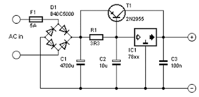
Parts List
R1 = 3.3 Ω 5 Watt
C1 = V 4700μF/63
C2 = V 10μF/35
C3 = 100nF
D1 = 35A
T1 = MJ2955 (TO220), MJE2955 (TO3), TIP2955 (TO247)
IC1 = 78xx
F1 = 5A
R1 = 3.3 Ω 5 Watt
C1 = V 4700μF/63
C2 = V 10μF/35
C3 = 100nF
D1 = 35A
T1 = MJ2955 (TO220), MJE2955 (TO3), TIP2955 (TO247)
IC1 = 78xx
F1 = 5A
Saturday, August 9, 2014
Build a Voltage to Frequency Converter Wiring diagram Schematic 3
Build a Voltage to Frequency Converter Circuit Diagram 3. The input voltage, V1, causes C1 to charge and produce a ramp voltage at the output of the 741 op amp. Diodes D1 and D2 are four-layer devices. When the voltage across C1 reaches the breakover voltage of either diode, the diode conducts to discharge C1 rapidly and the op amp output goes abruptly to zero. This rapid discharge action applies a narrow pulse to G1 and G2. Positive discharge pulses produced by a positive V1 are coupled to the output only through G1, while negative pulses are coupled only through G2.
Because of the forward break-over current of diodes D1 and D2, the schema won`t operate below a minimum input voltage. An increase of R1 increases this minimum voltage and reduces the schema`s dynamic range. The minimum input voltage with R1 at 1 Kn is in the range of 10 to 50 m V. This input dead zone, when input signal V1 is near zero is desirable in applications that require a signal to exceed a certain level before an output is generated.
Voltage to Frequency Converter Circuit Diagram 3

Friday, August 8, 2014
Build a Low Distortion Amplifier cum Compressor Wiring diagram Schematic
Build a Low Distortion Amplifier cum Compressor Circuit Diagram. Designers can build a 15-dB compressor with a miniature lamp and a current-feedback amplifier. The schema possesses extremely low distortion at frequencies above the lamp`s thermal time constant. This means that distortion is negligible from audio frequencies to beyond 10 MHz. There`s also relatively little change in phase versus gain compared to other automatic gain-control diagram. Lastly, the schema has many instrumentation, audio, and high-frequency applications as a result of its low distortion and small phase change.
The AD844 op amp is a perfect fit for this application because it`s a current-feedback amplifier. Each stage of the schema, U2, lamp, and feedback resistor compresses an ac signal by over 15 dB (see the figure). Cascading a number of stages delivers higher compression ranges. Op amp U1 operates as a unity-gain buffer to drive the input to the compressor. However, U1 is optional if a low-impedance signal source is used.
Low Distortion Amplifier cum Compressor Circuit Diagram
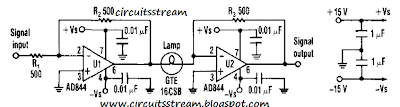
The lamp`s resistance will increase with temperature, which reduces the ratio of resistor R3 to the resistance of the lamp. This ratio reduces the gain of U2. The lamp`s cold resistance should be greater than the input resistance of U2 (more than 50 ) for proper operation. The lamp`s resistance will change slightly for low input levels. Therefore, the ratio of R3 to the resistance of the lamp and the gain of U2 stays high.
Subscribe to:
Posts (Atom)